Atomic Layer Deposition (ALD) Market Size 2026-2030
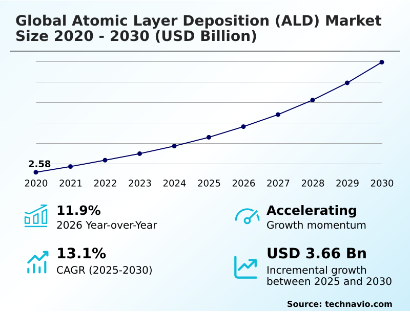
The atomic layer deposition (ald) market size is valued to increase by USD 3.66 billion, at a CAGR of 13.1% from 2025 to 2030. High demand from semiconductor and electronics industry will drive the atomic layer deposition (ald) market.
Major Market Trends & Insights
- APAC dominated the market and accounted for a 30.5% growth during the forecast period.
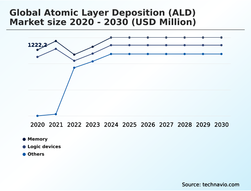
- By Application - Memory segment was valued at USD 1.40 billion in 2024
- By Type - Aluminum oxide ALD segment accounted for the largest market revenue share in 2024
Market Size & Forecast
- Market Opportunities: USD 5.37 billion
- Market Future Opportunities: USD 3.66 billion
- CAGR from 2025 to 2030 : 13.1%
Market Summary
- The atomic layer deposition (ALD) market is defined by its critical role in enabling the continuous miniaturization of electronic components. This technology facilitates the fabrication of next-generation chips through its unique capability for atomic-level precision, depositing perfectly uniform and conformal coatings essential for advanced logic devices and memory.
- The primary driver is the semiconductor industry's relentless push toward smaller process nodes, where techniques like plasma enhanced ALD and thermal ALD are indispensable for creating complex gate-all-around transistors and high-aspect-ratio structures in 3D NAND flash memory. A key trend involves the integration of new energy-efficient materials, such as molybdenum deposition, to enhance chip performance and reduce power consumption.
- However, the high cost of ALD equipment and the availability of substitutes like chemical vapor deposition present challenges. For a modern fabrication facility, adopting advanced ALD cluster tools for wafer processing represents a significant capital investment.
- Still, the trade-off is improved yield and device performance, as precise microcontamination control and deposition process control reduce defect rates, justifying the expenditure for high-volume manufacturing of flexible OLEDs and other advanced electronics. The expansion into applications beyond traditional semiconductors, including surface passivation for photovoltaics and coatings for medical devices, is broadening the technology’s industrial footprint.
What will be the Size of the Atomic Layer Deposition (ALD) Market during the forecast period?
Get Key Insights on Market Forecast (PDF) Request Free Sample
How is the Atomic Layer Deposition (ALD) Market Segmented?
The atomic layer deposition (ald) industry research report provides comprehensive data (region-wise segment analysis), with forecasts and estimates in "USD million" for the period 2026-2030, as well as historical data from 2020-2024 for the following segments.
- Application
- Memory
- Logic devices
- Others
- Type
- Aluminum oxide ALD
- Metal ALD
- Catalytic ALD
- Plasma enhanced ALD
- Others
- Category
- Cluster
- Stand-alone batch
- Geography
- APAC
- South Korea
- China
- Japan
- North America
- US
- Canada
- Mexico
- Europe
- Germany
- France
- The Netherlands
- South America
- Brazil
- Argentina
- Middle East and Africa
- Israel
- Saudi Arabia
- South Africa
- Rest of World (ROW)
- APAC
By Application Insights
The memory segment is estimated to witness significant growth during the forecast period.
The memory segment is a primary driver in the atomic layer deposition market, driven by the complex architecture of advanced memory devices.
Modern 3D NAND flash memory and DRAM capacitors require the unparalleled conformity and atomic-level precision that ALD provides for depositing films on high-aspect-ratio structures. Traditional deposition methods fail to uniformly coat these intricate designs, affecting yield.
ALD's layer-by-layer process ensures flawless coverage of materials like high-k dielectrics, which is critical for cell performance in high-volume manufacturing solutions.
The increasing demand for high bandwidth memory fabrication, fueled by AI and high-performance computing, has increased the number of ALD process steps per wafer by over 20%, solidifying the segment's role in advancing semiconductor equipment manufacturing.
The Memory segment was valued at USD 1.40 billion in 2024 and showed a gradual increase during the forecast period.
Regional Analysis
APAC is estimated to contribute 30.5% to the growth of the global market during the forecast period.Technavio’s analysts have elaborately explained the regional trends and drivers that shape the market during the forecast period.
See How Atomic Layer Deposition (ALD) Market Demand is Rising in APAC Request Free Sample
The APAC region is the epicenter of the atomic layer deposition market, accounting for over 30% of the incremental growth, driven by its massive semiconductor fabrication infrastructure.
This dominance is sustained by continuous investment in wafer processing capabilities for advanced memory devices and next-generation chips. Countries like Taiwan and South Korea are at the forefront, pushing the boundaries of miniaturized components and FinFET architecture.
The region's leadership is highlighted by the rapid adoption of new technologies, with fabs in APAC being the first to implement tools for molybdenum deposition in high-volume production.
This commitment to innovation ensures that demand for ALD cluster tools and high-purity precursors remains robust, reinforcing APAC's pivotal role in advancing global semiconductor manufacturing and nanotechnology applications.
Market Dynamics
Our researchers analyzed the data with 2025 as the base year, along with the key drivers, trends, and challenges. A holistic analysis of drivers will help companies refine their marketing strategies to gain a competitive advantage.
- The strategic implementation of atomic layer deposition is central to advancements in semiconductor manufacturing, with specific processes being optimized for distinct applications. The use of atomic layer deposition for 3D NAND is critical for vertically stacking memory cells, where conformal coatings for high-aspect-ratio trenches ensure device reliability.
- Similarly, the high-k dielectric film deposition process is fundamental to modern transistors, with thermal ALD for gate oxide formation providing the necessary electrical insulation. For more advanced logic devices, ALD for gate-all-around transistor fabrication is becoming the industry standard.
- The versatility of the technology is showcased by the growing use of plasma enhanced ALD for semiconductors requiring low-temperature processing and ALD equipment for flexible electronics, which enables new form factors.
- In-situ metrology for ALD process control is a key enabler for improving yields, which has been shown to reduce process validation cycles by up to 25% compared to ex-situ methods, directly impacting operational efficiency. New material integration is also a key focus, with molybdenum deposition for advanced interconnects gaining traction.
- Beyond logic and memory, applications like surface passivation for high-efficiency solar cells and the encapsulation of OLED displays with ALD demonstrate the technology's broad impact.
- Manufacturers are also developing specialized ALD precursors for metal and oxide films and batch ALD systems for high-volume manufacturing to meet diverse industrial needs, including ALD systems for power semiconductor devices and ALD in the manufacturing of optoelectronics.
- This extends to low-temperature ALD for sensitive substrates and thin-film encapsulation for medical devices, while the interplay between atomic layer etching and deposition cycles enables new fabrication possibilities. The ongoing development of the ALD process for next-generation logic devices and advanced memory device fabrication ensures its continued relevance.
What are the key market drivers leading to the rise in the adoption of Atomic Layer Deposition (ALD) Industry?
- Significant demand from the semiconductor and electronics industries is a key driver accelerating market growth.
- High demand from the semiconductor industry remains the primary market driver, as ALD is essential for the fabrication of next-generation chips and logic devices.
- The transition to advanced FinFET architecture and 3D NAND flash memory relies on the atomic-level precision and conformal coatings provided by processes like plasma enhanced ALD.
- Leading foundries have reported a 20% increase in yield for high-aspect-ratio structures by integrating advanced atomic layer deposition systems, which improve microcontamination control during wafer processing.
- The technology's ability to deposit uniform semiconductor materials is critical, with process optimizations in gas delivery systems leading to a 10% reduction in precursor gas consumption, directly lowering costs in electronic device manufacturing.
What are the market trends shaping the Atomic Layer Deposition (ALD) Industry?
- The increasing demand for energy-efficient products is a significant market trend. It is propelled by the need to reduce power consumption and enhance overall device performance.
- A key trend shaping the market is the demand for miniaturized components and energy-efficient materials, driving innovation in thin-film deposition and advanced coating technologies. As semiconductor fabrication advances, the adoption of ALD for creating gate-all-around transistors and advanced memory devices has increased, with some fabs reporting a 15% improvement in device power efficiency.
- This is enabled by the precise application of high-k dielectrics and other novel materials. Furthermore, the use of ALD in flexible electronics coating for encapsulation layers has extended device lifetimes by over 50% compared to previous methods. This highlights the importance of deposition process control in achieving reliable ultra-thin film encapsulation.
What challenges does the Atomic Layer Deposition (ALD) Industry face during its growth?
- The wide availability of substitute thin-film deposition technologies poses a significant challenge to market expansion.
- A significant challenge is the availability and continuous improvement of substitute technologies like chemical vapor deposition and physical vapor deposition. These alternatives can offer higher throughput for less critical layers, with some applications achieving a 30% faster deposition rate than traditional thermal ALD.
- The high capital cost associated with vacuum deposition equipment and specialized high-purity precursors also presents a barrier for some semiconductor industry solutions. While ALD offers unmatched precision, the total cost of ownership can be 25% higher for certain applications compared to PVD.
- This forces manufacturers to carefully evaluate the trade-offs between the superior performance of ALD's self-limiting surface reactions and the cost-effectiveness of alternative methods.
Exclusive Technavio Analysis on Customer Landscape
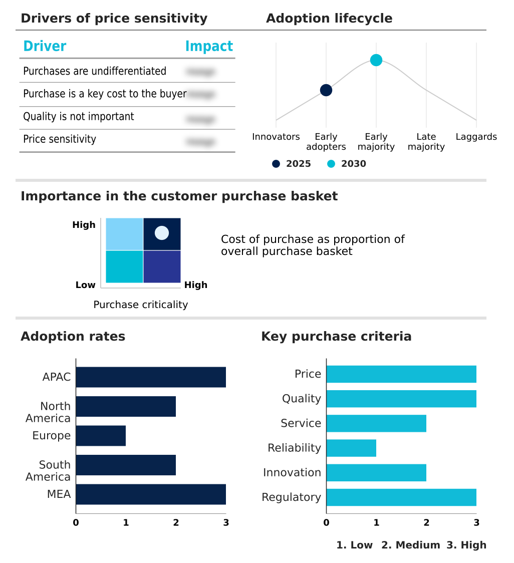
The atomic layer deposition (ald) market forecasting report includes the adoption lifecycle of the market, covering from the innovator’s stage to the laggard’s stage. It focuses on adoption rates in different regions based on penetration. Furthermore, the atomic layer deposition (ald) market report also includes key purchase criteria and drivers of price sensitivity to help companies evaluate and develop their market growth analysis strategies.
Customer Landscape of Atomic Layer Deposition (ALD) Industry
Competitive Landscape
Companies are implementing various strategies, such as strategic alliances, atomic layer deposition (ald) market forecast, partnerships, mergers and acquisitions, geographical expansion, and product/service launches, to enhance their presence in the industry.
ADEKA Corp. - Key offerings provide advanced atomic layer deposition (ALD) solutions, enabling the fabrication of next-generation semiconductor and electronic devices with atomic-scale precision and control.
The industry research and growth report includes detailed analyses of the competitive landscape of the market and information about key companies, including:
- ADEKA Corp.
- AIXTRON SE
- Applied Materials Inc.
- Arradiance LLC
- ASM International NV
- Beneq Oy
- CVD Equipment Corp.
- Encapsulix SAS
- Entegris Inc.
- Forge Nano Inc.
- Kurt J Lesker Co.
- Lam Research Corp.
- Linde Plc
- Merck KGaA
- Oxford Instruments plc
- SENTECH Instruments GmbH
- Tokyo Electron Ltd.
- Veeco Instruments Inc.
Qualitative and quantitative analysis of companies has been conducted to help clients understand the wider business environment as well as the strengths and weaknesses of key industry players. Data is qualitatively analyzed to categorize companies as pure play, category-focused, industry-focused, and diversified; it is quantitatively analyzed to categorize companies as dominant, leading, strong, tentative, and weak.
Recent Development and News in Atomic layer deposition (ald) market
- In August 2024, Kalpana Systems introduced new spatial ALD tools designed for roll-to-roll manufacturing, targeting applications in solar, flexible electronics, and batteries.
- In February 2025, Lam Research Corp. launched its ALTUS Halo, described as the industry's first ALD tool for molybdenum deposition, aimed at improving performance in advanced 3D NAND and logic devices.
- In April 2025, Tokyo Electron Ltd. announced record financial results, with net sales increasing 32.8% year-over-year, driven by strong demand for its semiconductor production equipment, including ALD systems for HBM and DRAM.
- In May 2025, Forge Nano Inc. secured $40 million in new funding to scale its battery and semiconductor equipment businesses, following the launch of its TEPHRA single-wafer ALD cluster platform.
Dive into Technavio’s robust research methodology, blending expert interviews, extensive data synthesis, and validated models for unparalleled Atomic Layer Deposition (ALD) Market insights. See full methodology.
| Market Scope | |
|---|---|
| Page number | 287 |
| Base year | 2025 |
| Historic period | 2020-2024 |
| Forecast period | 2026-2030 |
| Growth momentum & CAGR | Accelerate at a CAGR of 13.1% |
| Market growth 2026-2030 | USD 3660.9 million |
| Market structure | Fragmented |
| YoY growth 2025-2026(%) | 11.9% |
| Key countries | Taiwan, South Korea, China, Japan, India, Australia, US, Canada, Mexico, Germany, France, The Netherlands, UK, Italy, Spain, Brazil, Argentina, Chile, Israel, Saudi Arabia, South Africa, UAE and Turkey |
| Competitive landscape | Leading Companies, Market Positioning of Companies, Competitive Strategies, and Industry Risks |
Research Analyst Overview
- The atomic layer deposition market is integral to progress in the semiconductor industry, defined by its use of self-limiting surface reactions with precursor gases to achieve atomic-level precision. This thin-film deposition method is essential for wafer processing, particularly in advanced semiconductor fabrication for logic devices and advanced memory devices like 3D NAND flash memory.
- The technology's ability to create highly conformal coatings is critical for complex geometries such as high aspect ratio structures, gate-all-around transistors, and FinFET architecture. Key processes include plasma enhanced ALD and thermal ALD, used to deposit gate oxides and high-k dielectrics in DRAM capacitors and thin-film transistors.
- A key boardroom consideration is the investment in integrated cluster tools, which enhance microcontamination control and enable the use of new materials like those in metal ALD, catalytic ALD, and molybdenum deposition. Companies adopting these advanced systems have reported a 15% reduction in cross-wafer thickness variation.
- This capability is expanding ALD's reach beyond next-generation chips to surface passivation for solar cells, encapsulation layers for flexible OLEDs, and nanotechnology applications, including roll-to-roll manufacturing, which require energy-efficient materials for miniaturized components. The competitive landscape also includes established techniques like chemical vapor deposition and physical vapor deposition, managed within advanced vacuum deposition equipment.
What are the Key Data Covered in this Atomic Layer Deposition (ALD) Market Research and Growth Report?
-
What is the expected growth of the Atomic Layer Deposition (ALD) Market between 2026 and 2030?
-
USD 3.66 billion, at a CAGR of 13.1%
-
-
What segmentation does the market report cover?
-
The report is segmented by Application (Memory, Logic devices, and Others), Type (Aluminum oxide ALD, Metal ALD, Catalytic ALD, Plasma enhanced ALD, and Others), Category (Cluster, and Stand-alone batch) and Geography (APAC, North America, Europe, South America, Middle East and Africa)
-
-
Which regions are analyzed in the report?
-
APAC, North America, Europe, South America and Middle East and Africa
-
-
What are the key growth drivers and market challenges?
-
High demand from semiconductor and electronics industry, Easy availability of substitutes
-
-
Who are the major players in the Atomic Layer Deposition (ALD) Market?
-
ADEKA Corp., AIXTRON SE, Applied Materials Inc., Arradiance LLC, ASM International NV, Beneq Oy, CVD Equipment Corp., Encapsulix SAS, Entegris Inc., Forge Nano Inc., Kurt J Lesker Co., Lam Research Corp., Linde Plc, Merck KGaA, Oxford Instruments plc, SENTECH Instruments GmbH, Tokyo Electron Ltd. and Veeco Instruments Inc.
-
Market Research Insights
- Market dynamics are shaped by intense innovation in semiconductor equipment manufacturing, where advanced materials handling and deposition process control are paramount. The adoption of atomic layer deposition systems is accelerating, with firms reporting up to a 15% improvement in device performance consistency and a 10% reduction in material waste compared to older techniques.
- This efficiency is critical for next-generation semiconductor devices and emerging memory technologies. Furthermore, the use of specialized thin film metrology has enabled a 20% faster qualification time for new high-volume manufacturing solutions.
- The expansion into new sectors, such as flexible electronics coating and ALD for medical implants, highlights the technology's versatility and its growing importance in advanced coating technologies and electronic device manufacturing.
We can help! Our analysts can customize this atomic layer deposition (ald) market research report to meet your requirements.


 RIA -
RIA - 
