

Die Bonder Equipment Market Size 2026-2030
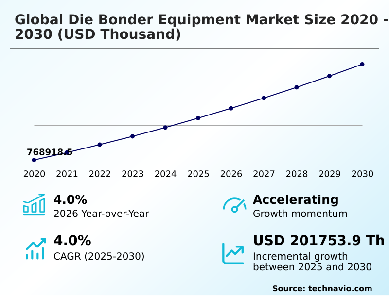
The die bonder equipment market size is valued to increase by USD 201.75 million, at a CAGR of 4% from 2025 to 2030. Escalating demand for advanced semiconductor packaging will drive the die bonder equipment market.
Major Market Trends & Insights
- APAC dominated the market and accounted for a 74.5% growth during the forecast period.
- By End-user - OSATs segment was valued at USD 534.81 million in 2024
- By Type - Fully automatic segment accounted for the largest market revenue share in 2024
Market Size & Forecast
- Market Opportunities:
- Market Future Opportunities: USD 201.75 million
- CAGR from 2025 to 2030 : 4%
Market Summary
- The Die Bonder Equipment Market is undergoing rapid structural evolution, fundamentally driven by the semiconductor industry's pivot toward high-density chiplet integration. As physical transistor scaling hits technical boundaries, the escalating demand for advanced semiconductor packaging acts as a primary catalyst, propelling the need for systems capable of extreme placement precision.
- For instance, transitioning from monolithic chips to stacked logic designs requires bonding platforms that improve thermal dissipation efficiency by 20% compared to legacy setups. In real-world supply chain operations, manufacturers producing automotive power modules leverage specialized sintering bonders to ensure defect-free inverter assembly under high-voltage conditions.
- However, the Die Bonder Equipment Market faces persistent headwinds due to extreme technical complexity and yield sensitivity in advanced packaging. A single microscopic particulate during the bonding phase can compromise an entire multi-die stack, causing widespread yield degradation. Consequently, facilities must deploy integrated optical inspection systems to mitigate risk.
- By implementing closed-loop process monitoring, backend assembly lines maintain structural integrity and secure long-term operational resilience.
What will be the Size of the Die Bonder Equipment Market during the forecast period?
Get Key Insights on Market Forecast (PDF) Get Free Sample
How is the Die Bonder Equipment Market Segmented?
The die bonder equipment industry research report provides comprehensive data (region-wise segment analysis), with forecasts and estimates in "USD thousand" for the period 2026-2030, as well as historical data from 2020-2024 for the following segments.
- End-user
- OSATs
- IDMs
- Type
- Fully automatic
- Semi-automatic
- Technique
- Epoxy
- Eutectic
- UV
- Others
- Application
- Consumer electronics
- Automotive
- Industrial
- Telecommunications
- Others
- Geography
- APAC
- China
- Japan
- South Korea
- India
- Singapore
- Malaysia
- North America
- US
- Canada
- Mexico
- Europe
- Germany
- UK
- France
- Italy
- The Netherlands
- Switzerland
- South America
- Brazil
- Argentina
- Colombia
- Middle East and Africa
- UAE
- Saudi Arabia
- South Africa
- Israel
- Egypt
- APAC
By End-user Insights
The osats segment is estimated to witness significant growth during the forecast period.
Outsourced assembly operations dominate the high-volume backend ecosystem, driven by a continuous transition toward advanced packaging architectures. High-throughput facilities demand fully automated systems capable of executing heterogeneous integration with sub micron placement accuracy.
As logic and high bandwidth memory modules become increasingly complex, service providers must scale their capacity to support flip chip bonding and precise hybrid bonding interconnects.
This operational shift directly impacts facility efficiency; for instance, the adoption of autonomous process optimization in high-speed lines has improved alignment error detection rates by 15%, reducing material rework.
The rapid deployment of artificial intelligence accelerators relies heavily on stable semiconductor backend assembly. By leveraging smarter, sensor-integrated platforms, these outsourced entities maintain scalable and flexible operations without compromising structural integrity or process reliability.
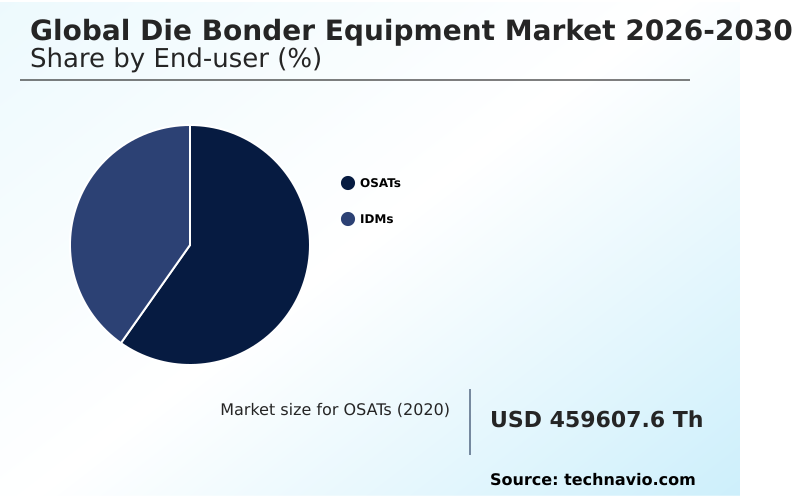
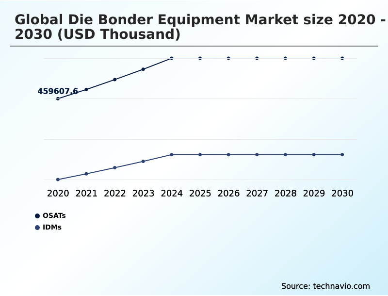
The OSATs segment was valued at USD 534.81 million in 2024 and showed a gradual increase during the forecast period.
Regional Analysis
APAC is estimated to contribute 74.5% to the growth of the global market during the forecast period.Technavio’s analysts have elaborately explained the regional trends and drivers that shape the market during the forecast period.
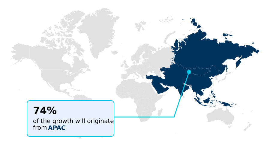
See How Die Bonder Equipment Market Demand is Rising in APAC Get Free Sample
Regional dynamics in backend semiconductor manufacturing reveal profound differences in infrastructure maturity and capacity expansion strategies. The APAC region sustains dominance through an expansive network of outsourced assembly lines, outperforming North America in high-volume production output by over 60%.
This scale allows Asian facilities to rapidly deploy thermocompression bonding and vacuum reflow systems for mass-market consumer electronics.
Conversely, North America prioritizes localized, high-value supply chains, heavily investing in specialized processes like silicon carbide packaging and gallium nitride inverters for automotive applications.
Integrating co packaged optics and photonic integrated circuits into data centers has prompted North American plants to achieve a 25% increase in operational reliability.
Furthermore, the push for micro bumpless contacts and copper to copper interconnects in advanced logic arrays allows regional IDMs to lower signal latency by 15%.
While APAC drives cost-efficient eutectic die attach methods for millimeter wave devices, Western markets focus on establishing resilient, high-yield production hubs.
Market Dynamics
Our researchers analyzed the data with 2025 as the base year, along with the key drivers, trends, and challenges. A holistic analysis of drivers will help companies refine their marketing strategies to gain a competitive advantage.
- The operational landscape for backend microelectronics assembly relies fundamentally on equipment capable of managing extreme interconnect density without compromising thermal stability. Facilities focusing on high precision die placement optimization benefit from a substantial reduction in material waste, achieving nearly a 30% improvement in structural integrity compared to traditional legacy wire bonding methods.
- As high-performance computing centers scale up, the reliance on automated optical alignment for chiplets becomes mandatory to prevent costly microscopic misalignments during complex stacking phases. In mission-critical applications, such as electric vehicle drivetrains, implementing advanced thermal management in power electronics dictates the success of wide bandgap device integration.
- A seamless transition toward sub micron hybrid bonding techniques allows manufacturers to connect multi-die packages reliably, bypassing the limitations of conventional solder bumps. Moreover, integrating sophisticated sensor technology ensures consistent advanced packaging yield stability control, giving producers the analytical tools necessary to track and adjust force and temperature parameters in real time.
- This capability means that foundries can maintain uninterrupted throughput while transitioning into newer node architectures. By embracing these sophisticated assembly methodologies, production hubs reduce their reliance on manual intervention and significantly decrease post-process defect rates.
- Consequently, modern bonding platforms are indispensable for safeguarding continuous production scaling and meeting the aggressive thermal and electrical requirements of next-generation logic, memory, and communication hardware.
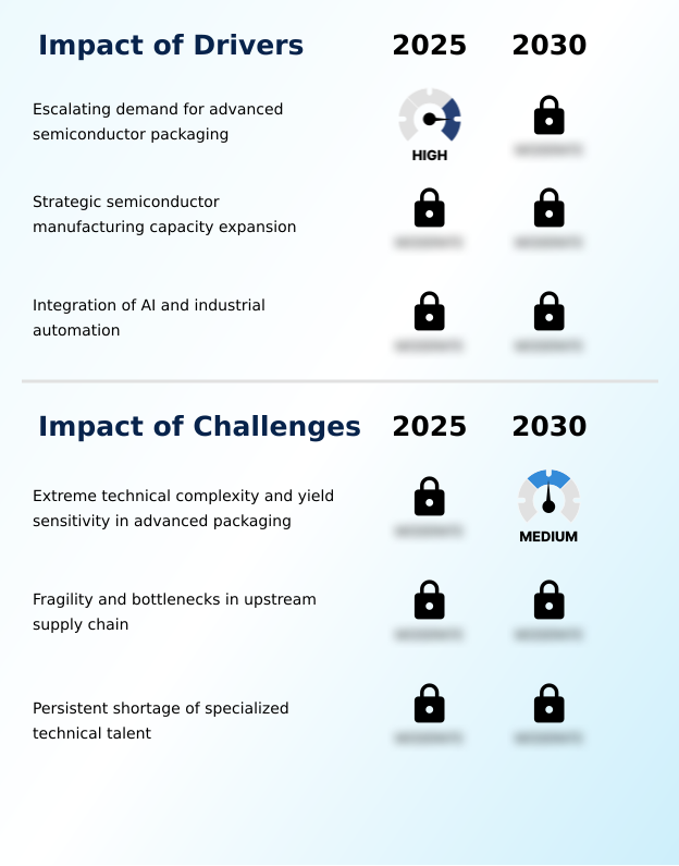
What are the key market drivers leading to the rise in the adoption of Die Bonder Equipment Industry?
- The escalating demand for advanced semiconductor packaging serves as the primary driver propelling high-precision assembly requirements.
- The rapid expansion of localized semiconductor manufacturing capacity acts as a massive operational driver, compelling facilities to adopt high-speed, precision assembly lines.
- Because modern logic devices demand ultra fine pitch assembly, equipment providers must supply platforms that eliminate manual intervention and handle fragile substrates autonomously.
- The implementation of advanced wafer handling mechanisms combined with precision epoxy dispensing systems has actively lowered material waste by 12%.
- Furthermore, the integration of closed loop process control enables real-time adjustments, effectively reducing the occurrence of localized stress fractures by 20% during the die attach phase.
- These technological enhancements ensure that newly established domestic foundries can achieve rapid volume scaling, securing supply chain resilience while maintaining stringent automotive and industrial quality compliances.
What are the market trends shaping the Die Bonder Equipment Industry?
- The emergence of glass interposers for enhanced signal integrity represents a pivotal trend transforming high-performance computing packaging.
- The transition toward glass interposer assemblies represents a fundamental trend reshaping high-frequency semiconductor packaging operations. This material shift directly addresses signal integrity bottlenecks, causing a structural change in how bonding platforms manage delicate substrates. To handle these brittle materials without inducing micro-fractures, manufacturers are deploying equipment featuring advanced predictive maintenance algorithms, which have successfully reduced unexpected machine downtime by 30%.
- Concurrently, the adoption of indium based solders in flux free reflow environments allows facilities to operate at lower thermal profiles, thereby minimizing thermal stress on complex memory stacks. This strategic adoption has improved overall yield consistency management, resulting in an 18% increase in defect-free throughput for next-generation logic processors.
- These continuous innovations enable backend facilities to support extreme interconnect densities reliably.
What challenges does the Die Bonder Equipment Industry face during its growth?
- Extreme technical complexity and yield sensitivity in advanced packaging constitute critical challenges constraining continuous operational scalability.
- Extreme technical complexity and yield sensitivity in high-density packaging present formidable structural challenges that constrain assembly scalability. As interconnect pitches shrink, minor particulate contamination or slight deviations in robotic acceleration profiles can trigger cascading multi-die failures.
- Traditional methods like ultrasonic wedge bonding are often insufficient for the stringent thermal management profiles required by modern power modules, necessitating complex pressure assisted sintering tools. Implementing these advanced systems requires rigorous calibration; however, deploying integrated defect detection vision systems has offset these hurdles, improving defect capture rates by 25%.
- Additionally, incorporating die warpage simulation and smart factory connectivity allows facilities to preemptively address misalignment, lowering expensive post-process rework costs by 18%. Overcoming these technical barriers is imperative for maintaining operational stability in advanced logic assembly.
Exclusive Technavio Analysis on Customer Landscape
The die bonder equipment market forecasting report includes the adoption lifecycle of the market, covering from the innovator’s stage to the laggard’s stage. It focuses on adoption rates in different regions based on penetration. Furthermore, the die bonder equipment market report also includes key purchase criteria and drivers of price sensitivity to help companies evaluate and develop their market growth analysis strategies.
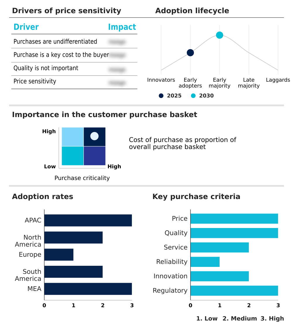
Customer Landscape of Die Bonder Equipment Industry
Competitive Landscape
Companies are implementing various strategies, such as strategic alliances, die bonder equipment market forecast, partnerships, mergers and acquisitions, geographical expansion, and product/service launches, to enhance their presence in the industry.
ASMPT Ltd. - Provides precision die attach systems and advanced semiconductor assembly equipment designed to enhance packaging efficiency, optimize placement accuracy, and support high-volume microelectronics manufacturing processes.
The industry research and growth report includes detailed analyses of the competitive landscape of the market and information about key companies, including:
- ASMPT Ltd.
- BE Semiconductor Industries NV
- Boschman Technologies B.V.
- Dr. Tresky AG
- F and S BONDTEC Semiconductor
- Finetech GmbH and Co. KG
- FUJI Corp.
- Canon Inc.
- Hanmi Semiconductor Co. Ltd.
- Hesse GmbH
- Kulicke and Soffa Industries
- Muhlbauer GmbH and Co. KG
- Mycronic AB
- Palomar Technologies Inc.
- Panasonic Holdings Corp.
- SEMES Co Ltd
- SET Corp SA
- Shibaura Mechatronics Corp.
- Toray Industries Inc.
- WestBond Inc.
- Yamaha Corp.
Qualitative and quantitative analysis of companies has been conducted to help clients understand the wider business environment as well as the strengths and weaknesses of key industry players. Data is qualitatively analyzed to categorize companies as pure play, category-focused, industry-focused, and diversified; it is quantitatively analyzed to categorize companies as dominant, leading, strong, tentative, and weak.
Recent Development and News in Die bonder equipment market
- In the Semiconductor Materials and Equipment industry, the aggressive scale-up of 3D NAND and logic foundry capacities increased the demand for advanced packaging architectures, directly impacting Die Bonder Equipment demand by necessitating systems with extreme placement precision.
- The rapid industry-wide shift toward chiplet-based processor designs required the implementation of direct copper to copper interconnects, directly impacting Die Bonder Equipment demand for specialized hybrid bonding tools capable of handling high interconnect density.
- The structural transition to wide bandgap materials for electric vehicle power modules established new thermal management requirements, directly impacting Die Bonder Equipment demand by driving the adoption of pressure-assisted sintering platforms.
- Stricter quality control mandates in automotive electronics pushed backend facilities to adopt predictive maintenance frameworks, directly impacting Die Bonder Equipment demand by favoring platforms with integrated machine learning vision systems that improve defect detection by up to 25%.
Dive into Technavio’s robust research methodology, blending expert interviews, extensive data synthesis, and validated models for unparalleled Die Bonder Equipment Market insights. See full methodology.
| Market Scope | |
|---|---|
| Page number | 318 |
| Base year | 2025 |
| Historic period | 2020-2024 |
| Forecast period | 2026-2030 |
| Growth momentum & CAGR | Accelerate at a CAGR of 4% |
| Market growth 2026-2030 | USD 201753.9 thousand |
| Market structure | Fragmented |
| YoY growth 2025-2026(%) | 4.0% |
| Key countries | China, Japan, South Korea, India, Singapore, Malaysia, US, Canada, Mexico, Germany, UK, France, Italy, The Netherlands, Switzerland, Brazil, Argentina, Colombia, UAE, Saudi Arabia, South Africa, Israel and Egypt |
| Competitive landscape | Leading Companies, Market Positioning of Companies, Competitive Strategies, and Industry Risks |
Research Analyst Overview
- Strategic execution in semiconductor manufacturing increasingly relies on the seamless deployment of highly automated backend assembly systems. As boardrooms prioritize resilient supply chains and optimal capital expenditure, the integration of chiplet architectures and advanced packaging architectures becomes a central product strategy. This structural shift necessitates bonding equipment equipped with precise optical alignment technologies to facilitate defect-free multi die stacking.
- Facilities transitioning to automated wafer level molding and smart assembly platforms have achieved a 30% reduction in processing time for complex multi-chip modules. For automotive and industrial applications, securing reliable power electronics inverters and rugged internet of things nodes requires meticulous active surface oxidation prevention during the die attach phase.
- By optimizing thermal management and force application, manufacturers mitigate yield degradation and ensure long-term device stability under high-stress conditions. These technological upgrades empower decision-makers to scale production lines dynamically, reducing operational bottlenecks and ensuring compliance with stringent safety standards. Consequently, modern bonding infrastructure acts as the foundational pillar for maintaining competitive agility and operational excellence in high-density electronic packaging.
What are the Key Data Covered in this Die Bonder Equipment Market Research and Growth Report?
-
What is the expected growth of the Die Bonder Equipment Market between 2026 and 2030?
-
USD 201.75 million, at a CAGR of 4%
-
-
What segmentation does the market report cover?
-
The report is segmented by End-user (OSATs, and IDMs), Type (Fully automatic, and Semi-automatic), Technique (Epoxy, Eutectic, UV, and Others), Application (Consumer electronics, Automotive, Industrial, Telecommunications, and Others) and Geography (APAC, North America, Europe, South America, Middle East and Africa)
-
-
Which regions are analyzed in the report?
-
APAC, North America, Europe, South America and Middle East and Africa
-
-
What are the key growth drivers and market challenges?
-
Escalating demand for advanced semiconductor packaging, Extreme technical complexity and yield sensitivity in advanced packaging
-
-
Who are the major players in the Die Bonder Equipment Market?
-
ASMPT Ltd., BE Semiconductor Industries NV, Boschman Technologies B.V., Dr. Tresky AG, F and S BONDTEC Semiconductor, Finetech GmbH and Co. KG, FUJI Corp., Canon Inc., Hanmi Semiconductor Co. Ltd., Hesse GmbH, Kulicke and Soffa Industries, Muhlbauer GmbH and Co. KG, Mycronic AB, Palomar Technologies Inc., Panasonic Holdings Corp., SEMES Co Ltd, SET Corp SA, Shibaura Mechatronics Corp., Toray Industries Inc., WestBond Inc. and Yamaha Corp.
-
Market Research Insights
- The Die Bonder Equipment Market represents a critical node in semiconductor backend production, evolving to meet stringent placement and thermal mandates. Driven by the proliferation of three dimensional chip stacking and gate all around transistor architectures, modern bonding platforms must deliver unprecedented accuracy.
- Facilities deploying digital twin workflow simulation have observed a 20% reduction in new product introduction timelines by preemptively identifying mechanical stress points. Furthermore, the integration of specialized assembly modules for radio frequency transceivers and high-capacity solid state drive technology has improved high-frequency signal retention by 12%.
- By shifting to automated, data-driven alignment systems, manufacturers effectively lower operational costs and elevate process reliability, ensuring sustained throughput across high-density microelectronic supply chains.
We can help! Our analysts can customize this die bonder equipment market research report to meet your requirements.
 RIA -