Electron Microscope Market Size 2025-2029
The electron microscope market size is forecast to increase by USD 1.97 billion at a CAGR of 8.5% between 2024 and 2029.
- The market is witnessing significant growth due to the increasing demand for root-cause failure analysis in various industries, particularly in semiconductor manufacturing and material science research. This trend is driven by the need to enhance product quality, improve performance, and ensure product safety and reliability. Moreover, the increasing demand for Large-Volume Electron Microscopes (LVEMs) is fueling market growth, as these microscopes offer higher throughput and improved imaging capabilities. However, the market faces challenges, including the high cost of electron microscopes and heavy excise duties, which limit the adoption of these technologies, especially for small and medium-sized enterprises.
- To capitalize on market opportunities, companies should focus on developing cost-effective solutions and collaborating with governments to reduce excise duties. Effective strategic planning and operational efficiency are essential for companies seeking to navigate these challenges and maintain a competitive edge in the market.
What will be the Size of the Electron Microscope Market during the forecast period?

- The market continues to evolve, driven by advancements in material characterization techniques and their applications across various sectors. Integrated circuits, surface morphology, environmental science, and atomic resolution are key areas of focus. In-situ experiments enable the study of dynamic processes, providing valuable insights into materials science. Biocompatible materials and advanced materials find extensive use in cellular imaging, drug discovery, tissue engineering, and quality control. Clinical diagnostics, failure analysis, and imaging techniques are crucial in various industries. Particle analysis, thin films, and focused ion beam are essential tools for nanoparticle characterization and life sciences research.
- Defect analysis, microfluidic devices, and corrosion analysis are also significant applications. Electron tomography and cryo-electron microscopy offer new possibilities in material science research. The market's continuous unfolding is shaped by ongoing research and development, including sample preparation, electron beam, elemental analysis, and microstructural analysis.
How is this Electron Microscope Industry segmented?
The electron microscope industry research report provides comprehensive data (region-wise segment analysis), with forecasts and estimates in "USD million" for the period 2025-2029, as well as historical data from 2019-2023 for the following segments.
- Application
- Semiconductors
- Life sciences
- Material sciences
- Nanotechnology
- Technology
- SEM
- TEM
- DBEM
- End-user
- Industries
- Institutions
- Others
- Geography
- North America
- US
- Canada
- Europe
- France
- Germany
- UK
- APAC
- Australia
- China
- India
- Japan
- South Korea
- Rest of World (ROW)
- North America
By Application Insights
The semiconductors segment is estimated to witness significant growth during the forecast period.
The market has experienced significant growth due to its application in various industries, particularly in materials science and semiconductors. In materials science, electron microscopes are utilized for microstructural analysis, surface morphology studies, and defect analysis of advanced materials, including biocompatible materials and nanoparticles. In the field of semiconductors, the increasing focus on miniaturization and the production of advanced components has led to a higher demand for electron microscopes. These tools are essential for research and development, in-situ experiments, and quality control in the semiconductor industry, where the reduction of node widths necessitates a more precise inspection process. Moreover, electron microscopes play a crucial role in other sectors such as forensic science, polymer science, tissue engineering, drug discovery, and clinical diagnostics.
In forensic science, these microscopes aid in failure analysis and imaging techniques for crime scene investigations. In polymer science, electron microscopes are used for nanoparticle characterization and understanding the microstructure of materials. In tissue engineering and drug discovery, electron microscopes enable cellular imaging and the analysis of tissue morphology. In clinical diagnostics, they are employed for particle analysis and material characterization, contributing to the development of new diagnostic tools. Electron microscopes are also used in various research areas, including environmental science, corrosion analysis, and electron tomography. These tools provide atomic resolution imaging, allowing researchers to study the structure and behavior of materials at the nanoscale level.
In addition, they are instrumental in the development and characterization of thin films, focused ion beams, and microfluidic devices. In the field of biomedical research and biomedical engineering, electron microscopes are essential for the study of biological structures and the development of new materials for medical applications. They are used for imaging cells, tissues, and biomaterials, providing valuable insights into their structure and function. Furthermore, electron microscopes are used in the analysis of materials for medical implants and biocompatible materials, ensuring their safety and effectiveness. In summary, the market is driven by its applications in various industries, including materials science, semiconductors, forensic science, polymer science, tissue engineering, drug discovery, clinical diagnostics, and research and development.
These tools provide valuable insights into the structure and behavior of materials at the nanoscale level, enabling advancements in technology and scientific research.
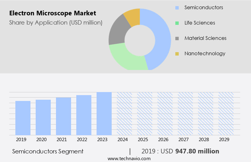
The Semiconductors segment was valued at USD 947.80 billion in 2019 and showed a gradual increase during the forecast period.
Regional Analysis
APAC is estimated to contribute 54% to the growth of the global market during the forecast period.Technavio’s analysts have elaborately explained the regional trends and drivers that shape the market during the forecast period.

The market is witnessing significant growth due to the increasing demand for advanced materials and nanotechnology in various industries. In materials science, electron microscopes are utilized for microstructural analysis, surface morphology studies, and defect analysis. The use of electron microscopes in polymer science and ceramic science enables the characterization of materials at the atomic level. In the field of life sciences, electron microscopes play a crucial role in cellular imaging, drug discovery, and tissue engineering. Forensic science benefits from electron microscopes for particle analysis and failure analysis. In-situ experiments and electron tomography are essential techniques used in research and development of advanced materials.
The integration of electron microscopes in dynamic processes such as corrosion analysis, environmental science, and quality control in industries like semiconductors and biomedical research is driving market growth. The adoption of electron microscopes in the characterization of thin films, focused ion beam, and nanoparticle characterization is also contributing to market expansion. The use of electron microscopes in microfluidic devices and transmission electron microscopes is further propelling market growth. The APAC region, with its large consumer base and high number of manufacturing firms, is a significant market for electron microscopes. The region's growing investments in infrastructure development and the modernization of small- and medium-sized enterprises have led to increased adoption of electron microscopes for various applications.
The demand for electron microscopes is also driven by the increasing focus on research and development in the field of materials science and nanotechnology.
Market Dynamics
Our researchers analyzed the data with 2024 as the base year, along with the key drivers, trends, and challenges. A holistic analysis of drivers will help companies refine their marketing strategies to gain a competitive advantage.
What are the key market drivers leading to the rise in the adoption of Electron Microscope Industry?
- The increasing demand for identifying the root causes of product or system failures is a primary market driver, necessitating the use of advanced root-cause failure analysis techniques and solutions.
- The market has gained significant traction in various industries, including ceramic science, materials science, polymer science, and forensic science. These microscopes offer high-resolution imaging and in-depth analysis of materials at the micro and nano levels, which is essential for understanding the structure and properties of advanced materials. In particular, the semiconductor industry and embedded systems have experienced a surge in complexity, leading to the need for more precise and accurate analysis tools. Scanning electron microscopes (SEMs) have become indispensable in this regard, providing superior resolution and precision compared to optical microscopes. SEMs utilize electron beams to analyze the surface of materials, revealing intricate details that are not visible with optical microscopes.
- This level of detail is crucial for the development of high-density products, such as high-end integrated circuits and printed circuit boards (PCBs), which require in-situ experiments to study dynamic processes. Moreover, SEMs are increasingly being used in fields like biocompatible materials and advanced materials research, where understanding the microstructure is vital for optimizing performance and ensuring quality. Electron backscatter diffraction (EBSD) is a powerful technique used in conjunction with SEMs to analyze crystal structures and determine their orientation, making it an essential tool for materials scientists and engineers. Overall, the market is poised for continued growth, driven by the increasing demand for high-performance materials and the need for more precise and accurate analysis tools.
What are the market trends shaping the Electron Microscope Industry?
- The professional trend in the market is marked by an escalating demand for Light Rail Vehicles (LRVs) or Light Rapid Transit Systems. This increasing requirement for efficient and sustainable public transportation solutions underscores the significance of LRVs in modern mobility solutions.
- Electron microscopes are essential tools for cellular imaging, drug discovery, tissue engineering, quality control, clinical diagnostics, failure analysis, and particle analysis. Low-voltage electron microscopes (LVEMs), which operate at a much lower voltage (less than 25kV) than high-voltage electron microscopes (HVEMs), offer several advantages. LVEMs are compact and can be used as desktop or tabletop models, making them suitable for various lab settings. They consume less space, cost less, and require minimal maintenance. Despite the lower resolution compared to HVEMs, LVEMs provide high contrast, which can be enhanced through hollow cone illumination or spherical aberration correction.
- In contrast, HVEMs can cause significant damage to specimens, especially for materials like polymers, composite materials, pigments, minerals, cells, and membranes due to the high radiation accumulation. LVEMs are particularly useful for imaging thin films and conducting focused ion beam (FIB) operations. FIB is a versatile technique used for material modification, sample preparation, and three-dimensional imaging. LVEMs with FIB capabilities enable precise material manipulation and characterization, making them indispensable in various industries, including electronics, materials science, and biology.
What challenges does the Electron Microscope Industry face during its growth?
- The escalating product costs and burdensome excise duties pose a significant challenge to the industry's growth trajectory.
- The market is driven by the need for material characterization in various industries, including material science, semiconductors, and environmental science. Electron microscopes are essential tools for understanding surface morphology, atomic resolution, and defect analysis in these fields. In research and development, electron tomography and nanoparticle characterization are crucial applications. The life sciences sector also relies on electron microscopes for studying biological structures at the molecular level. Despite the high initial investment required, the demand for electron microscopes remains steady due to their indispensable role in scientific research. However, the market growth is influenced by funding to research institutions, which can be unpredictable.
- Government and corporate funding play a significant role in the sale of electron microscopes. However, import duties and other taxes can increase the final price of the product, posing a challenge for market growth. In conclusion, the market is driven by the need for material characterization and research in various industries. However, the market growth is dependent on funding to research institutions and subject to import duties and other taxes. The uncertainty surrounding funding and the additional costs due to taxes create challenges for market growth.
Exclusive Customer Landscape
The electron microscope market forecasting report includes the adoption lifecycle of the market, covering from the innovator’s stage to the laggard’s stage. It focuses on adoption rates in different regions based on penetration. Furthermore, the electron microscope market report also includes key purchase criteria and drivers of price sensitivity to help companies evaluate and develop their market growth analysis strategies.

Customer Landscape
Key Companies & Market Insights
Companies are implementing various strategies, such as strategic alliances, electron microscope market forecast, partnerships, mergers and acquisitions, geographical expansion, and product/service launches, to enhance their presence in the industry.
Advantest Corp. - The company specializes in advanced electron microscopy solutions, including the MASK MVM-SEM E3600 series. These microscopes deliver high-resolution imaging and analysis capabilities, enabling researchers to explore materials at the nanoscale level. With cutting-edge technology and user-friendly design, these instruments facilitate breakthrough discoveries and innovations across various industries. By combining exceptional image quality, versatile functionality, and intuitive operation, the company's electron microscopes empower scientists to unlock new insights and advance their research objectives.
The industry research and growth report includes detailed analyses of the competitive landscape of the market and information about key companies, including:
- Advantest Corp.
- Agilent Technologies Inc.
- Bruker Corp.
- Carl Zeiss AG
- COXEM Co. Ltd.
- Danaher Corp.
- DELONG INSTRUMENTS AS
- Hirox Co. Ltd.
- HOVERLABS
- JEOL Ltd.
- Keysight Technologies Inc.
- Nikon Corp.
- Nion
- Novartis AG
- Olympus Corp.
- Seiko Holdings Corp.
- TESCAN GROUP
- Thermo Fisher Scientific Inc.
- Topcon Corp.
- UNISOKU Co. Ltd.
Qualitative and quantitative analysis of companies has been conducted to help clients understand the wider business environment as well as the strengths and weaknesses of key industry players. Data is qualitatively analyzed to categorize companies as pure play, category-focused, industry-focused, and diversified; it is quantitatively analyzed to categorize companies as dominant, leading, strong, tentative, and weak.
Recent Development and News in Electron Microscope Market
- In February 2023, Thermo Fisher Scientific, a leading life sciences solutions provider, announced the launch of its new Helion NanoLab 660 DualBeam FIB-SEM system. This advanced electron microscope integrates focused ion beam (FIB) milling and scanning electron microscopy (SEM) capabilities, enabling researchers to perform complex sample preparation and imaging tasks in a single instrument (Thermo Fisher Scientific press release, 2023).
- In July 2024, Hitachi High-Technologies Corporation and IBM Research entered into a strategic partnership to develop advanced electron microscopes using AI and machine learning technologies. The collaboration aims to improve the efficiency and accuracy of electron microscopy data analysis, which is crucial for material science, semiconductor, and life sciences research (Hitachi High-Technologies Corporation press release, 2024).
- In November 2024, FEI Company, a subsidiary of Thermo Fisher Scientific, received a significant order from the European Synchrotron Radiation Facility (ESRF) for a Titan Themis Z electron microscope. The instrument, valued at â¬13 million, will be used for advanced materials and life sciences research, strengthening ESRF's position as a leading European research facility (FEI Company press release, 2024).
- In March 2025, Tesla, Inc. Unveiled its new in-house developed Tesla Semiconductor Corporation, which includes a state-of-the-art electron microscope facility. The facility is designed to support the development and manufacturing of advanced semiconductor components, furthering Tesla's ambitions in the electric vehicle and renewable energy markets (Tesla, Inc. Press release, 2025).
Research Analyst Overview
The market is experiencing significant advancements, driven by the demand for sub-nanometer resolution and high-throughput screening. Electron guns power these microscopes, enabling nanoscale imaging and analysis of various materials. Virtual microscopy and machine learning are revolutionizing the field, allowing for remote access and automated data analysis. In-situ TEM and environmental TEM are essential for studying materials under real-world conditions. Composition analysis, phase identification, and chemical analysis are crucial components of electron microscopy, enhanced by machine learning and artificial intelligence. Data visualization and image segmentation facilitate 3D imaging and multimodal imaging, while electron holography and image processing offer improved accuracy.
Deep learning and automated microscopy enable faster and more precise analysis, and digital microscopy and field emission guns broaden the scope of applications. The integration of machine learning, artificial intelligence, and data analysis software enhances microscopy capabilities, providing valuable insights for US businesses.
Dive into Technavio’s robust research methodology, blending expert interviews, extensive data synthesis, and validated models for unparalleled Electron Microscope Market insights. See full methodology.
|
Market Scope |
|
|
Report Coverage |
Details |
|
Page number |
226 |
|
Base year |
2024 |
|
Historic period |
2019-2023 |
|
Forecast period |
2025-2029 |
|
Growth momentum & CAGR |
Accelerate at a CAGR of 8.5% |
|
Market growth 2025-2029 |
USD 1969.8 million |
|
Market structure |
Fragmented |
|
YoY growth 2024-2025(%) |
7.7 |
|
Key countries |
US, China, Japan, India, South Korea, Canada, Australia, UK, Germany, and France |
|
Competitive landscape |
Leading Companies, Market Positioning of Companies, Competitive Strategies, and Industry Risks |
What are the Key Data Covered in this Electron Microscope Market Research and Growth Report?
- CAGR of the Electron Microscope industry during the forecast period
- Detailed information on factors that will drive the growth and forecasting between 2025 and 2029
- Precise estimation of the size of the market and its contribution of the industry in focus to the parent market
- Accurate predictions about upcoming growth and trends and changes in consumer behaviour
- Growth of the market across APAC, North America, Europe, Middle East and Africa, and South America
- Thorough analysis of the market’s competitive landscape and detailed information about companies
- Comprehensive analysis of factors that will challenge the electron microscope market growth of industry companies
We can help! Our analysts can customize this electron microscope market research report to meet your requirements.