Focused Ion Beam Market Size 2024-2028
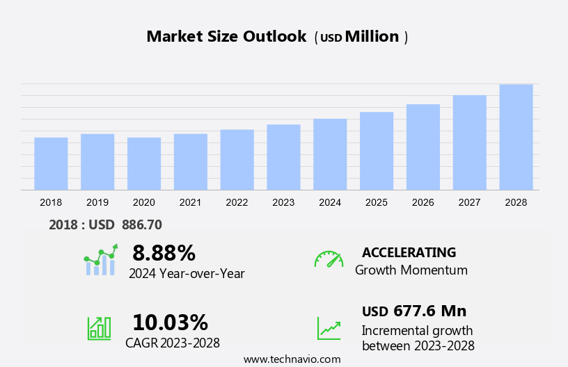
The focused ion beam market size is forecast to increase by USD 677.6 mn at a CAGR of 10.03% between 2023 and 2028.
- The focused ion beam (FIB) market is experiencing significant growth due to the increasing emphasis on nanotechnology and its applications in various industries. One notable trend is the use of FIB in gold nanofabrication for drug delivery in cancer treatment. This innovative approach offers precise control over the size and shape of nanoparticles, enhancing their therapeutic efficacy. However, the market also faces challenges related to toxicity concerns surrounding the use of gold nanofabrication in FIB systems. Addressing these issues through research and development of safer alternatives is crucial for the market's continued growth. Overall, the FIB market holds immense potential, driven by advancements in nanotechnology and the increasing demand for more precise and effective medical treatments.
What will be the Size of the Focused Ion Beam Market During the Forecast Period?
- The Focused Ion Beam (FIB) market encompasses systems utilized in various sectors, including semiconductor manufacturing, research laboratories, manufacturing firms, and institutes and universities. These systems employ ion beams to modify, analyze, and repair materials at the nanoscale, catering to the needs of the material science industry, physics, chemistry, engineering, and biomaterials. Applications span from circuit modification and layout verification to microcircuit failure analysis, mask repair, semiconductor device packaging, and display failure analysis. FIB systems are integral to the production of advanced technologies, such as nanomaterials, organic materials, smart materials, and ion beam lithography. The market is driven by the increasing demand for miniaturization, precision, and advanced materials in industries like semiconductors, life sciences, and precision machining tools. The market's growth is fueled by continuous innovation in FIB technology, including dualbeam systems and scanning electron microscopes.
How is this Focused Ion Beam Industry segmented and which is the largest segment?
The focused ion beam industry research report provides comprehensive data (region-wise segment analysis), with forecasts and estimates in "USD million" for the period 2024-2028, as well as historical data from 2018-2022 for the following segments.
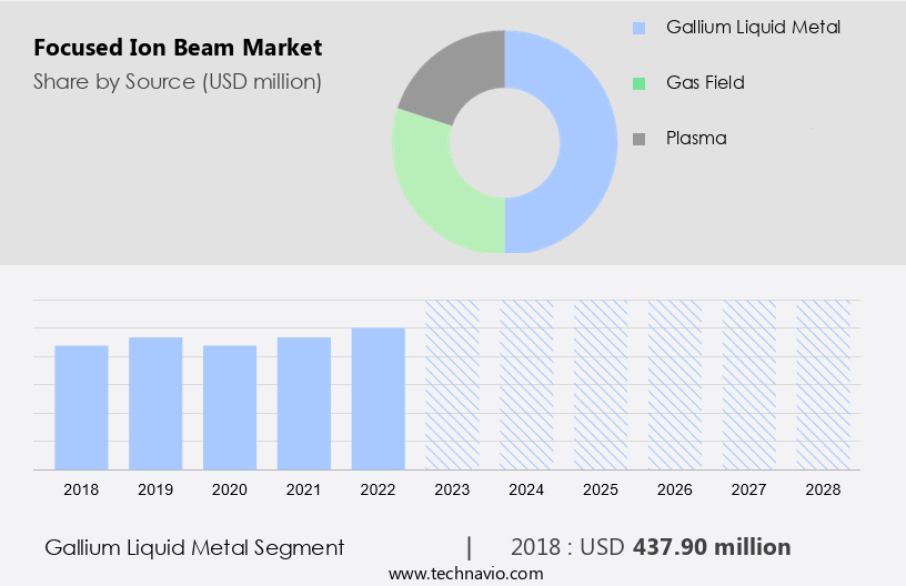
- Source
- Gallium liquid metal
- Gas field
- Plasma
- Geography
- North America
- US
- Europe
- Germany
- UK
- APAC
- Japan
- Middle East and Africa
- South America
- North America
By Source Insights
The gallium liquid metal segment is estimated to witness significant growth during the forecast period. Focused Ion Beams (FIB) utilize liquid metal ion sources (LMIS), such as gallium ions, for precision machining tool and materials analysis in various industries. Gallium is preferred due to its low melting point, inert nature, and suitable ion mass for milling. In semiconductor manufacturing, FIB is employed for circuit modification, layout verification, mask repair, and site-specific analysis. In physics and chemistry, FIB is used for thin films deposition, 3D visualization, and material science research. In biology, FIB is applied for cell morphology studies, biotechnology, and nanoscale machining of biological samples. FIB is also used in electronics and semiconductor industries for IC repair, electronics component manipulation, and electrical connections fabrication.
Additionally, FIB is used in cryogenic applications, dual beam SEM, environmental SEM, TEM sample preparation, and 3D reconstruction. The LMIS produces ions through electrospraying, with a strong electric field creating a Taylor cone at the tip, resulting in field evaporation and ion generation.
Get a glance at the market report of various segments Request Free Sample
The Gallium liquid metal segment was valued at USD 437.90 mn in 2018 and showed a gradual increase during the forecast period.
Regional Analysis
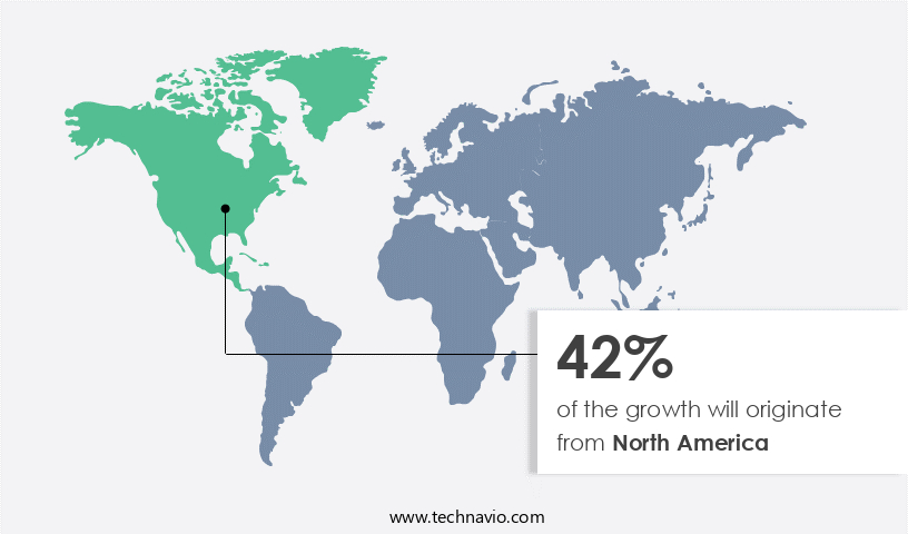
North America is estimated to contribute 42% to the growth of the global market during the forecast period. Technavio's analysts have elaborately explained the regional trends and drivers that shape the market during the forecast period.
For more insights on the market size of various regions, Request Free Sample
The Focused Ion Beam (FIB) market in North America is experiencing significant growth, with the US being the largest market in the region. The demand for FIBs is driven by the increasing activities in material sciences, nanotechnology, life sciences, and biotechnology sectors in the US. Semiconductor manufacturing is also a major contributor to the market, with some manufacturers considering setting up their bases in Mexico due to favorable labor costs and government initiatives. This will increase the demand for FIB-SEMs in the region for semiconductor manufacturing, IC repair, and material analysis applications. Canada and Mexico are other significant contributors to the market growth in North America.
The FIB market in North America caters to various industries, including semiconductor manufacturing, physics, chemistry, engineering, biomaterials, nanomaterials, organic materials, smart materials, and electronics. Applications of FIB include 3D visualization, circuit modification, layout verification, mask repair, nanoscale machining, and site-specific analysis. FIB is used for precision machining, milling, deposition, and micromachining of various materials, including silicon, Indium phosphide, Gallium arsenide, metal, porous materials, and thin films. FIB-SEMs are essential tools for the preparation of TEM specimens, 3D reconstruction, and porous materials characterization. The market for FIB is expected to grow due to the increasing demand for advanced materials and devices, automation, and robotics in various industries.
Market Dynamics
Our researchers analyzed the data with 2023 as the base year, along with the key drivers, trends, and challenges. A holistic analysis of drivers will help companies refine their marketing strategies to gain a competitive advantage.
What are the key market drivers leading to the rise in the adoption of Focused Ion Beam Industry?
- Increasing focus on nanotechnology is the key driver of the market.Nanotechnology, which encompasses materials sized between 1 and 100 nanometers, necessitates the use of Focused Ion Beams (FIB) systems and scanning electron microscopes. These advanced tools enable atomic and molecular-level analysis, essential for determining structure and texture properties. Nanotechnology's influence extends to altering atoms' core properties and characteristics through nanoscience applications. Governments and technology firms worldwide invest substantially in nanotechnology due to its expanding reach across sectors, including food, medicine, biomaterials, electronics, and microfabrication. In semiconductor manufacturing, FIB systems play a crucial role in nanoscale machining, masking, IC repairing applications, and material analysis. Nanomaterials such as silicon, indium phosphide, gallium arsenide, and various metals are subjected to FIB processes for thin films deposition, devices fabrication, and 3D visualization.
FIB systems facilitate site-specific analysis, circuit modification, and layout verification, while ion beam lithography offers mask repair and nanoscale precision machining. These advancements contribute significantly to the development of porous materials, solid state nanopores, and mesopores/macropores, providing insights into their transport properties and formation mechanisms. In the realm of biotechnology, FIB systems enable 3D reconstruction of cell morphology and TEM specimen preparation, while FIB SEM tomography offers valuable information on biological samples. FIB systems also play a role in electronics and semiconductor industries for cryogenic applications, dual beam SEM, environmental SEM, and transmission electron microscopy sample preparation. FIB systems' versatility extends to various applications, including circuit editing, gallium ion beam usage for TEM specimen preparation, plasma ion source integration, and ion source customization for integrated circuit repair and materials analysis.
Ion microscopy, direct write applications, and submicron level manipulation further expand FIB systems' scope.
What are the market trends shaping the Focused Ion Beam market?
- Use of gold nanofabrication for drug delivery in cancer treatment is the upcoming market trend.Focused Ion Beam (FIB) technology plays a pivotal role in the semiconductor manufacturing industry, particularly in the realm of physics, chemistry, and engineering. It finds extensive applications in the fabrication and modification of various materials, including silicon, indium phosphide, gallium arsenide, metals, and nanomaterials such as organic materials, smart materials, and porous materials. In the field of electronics and semiconductor industry, FIB is used for 3D visualization, processors, circuit modification, layout verification, mask repair, and IC repairing applications. FIB systems enable nanoscale machining, allowing for precise milling, deposition, and manipulation of materials at the submicron level. They are also used in material science and life science for site-specific analysis, imaging, and ion beam lithography.
FIB is instrumental in the formation mechanisms of solid state nanopores, thin films, and mesopores and macropores in porous materials. FIB SEM tomography is used for 3D reconstruction, providing valuable insights into the transport properties and structure of materials. FIB is also employed in the biotechnology sector for cell morphology analysis and sample preparation for Transmission Electron Microscopy (TEM) and Scanning Electron Microscope (SEM). In addition, FIB is used for cryogenic applications, environmental SEM, TEM specimen preparation, and 3D reconstruction. FIB systems use gallium ions beams and plasma ion sources for precision machining and ion microscopy. They are used in direct write applications, maskless implantation, and ion beam lithography for circuit editing and mask repair. FIB technology is a valuable tool in the semiconductor industry for electrical connections, conductive material manipulation, and computer chip repair.
What challenges does the Focused Ion Beam Industry face during its growth?
- Growing concerns about toxicity-related issues around gold nanofabrication for focused ion beam is a key challenge affecting the industry growth.The Focused Ion Beam (FIB) market encompasses applications in semiconductor manufacturing, physics, chemistry, engineering, biomaterials, nanomaterials, organic materials, and smart materials. FIB is utilized for various purposes such as semiconductor manufacturing, nanoscale machining, masking, IC repairing applications, and biological samples analysis in electronics and semiconductor industries. In the realm of material science and life science, FIB is employed for circuit modification, layout verification, mask repair, nanoscale, and direct write applications. FIB is used to manipulate and deposit materials at the nanoscale level, including silicon, indium phosphide, gallium arsenide, metal, and solid state nanopores. Thin films, devices, 3D visualization, processors, cell morphology, and porous materials are other areas where FIB finds extensive application.
FIB SEM tomography is used for 3D reconstruction, porosity characterization, and transport properties analysis. FIB is also used for site-specific analysis, imaging, milling, deposition, micromachining, and manipulation. Gallium ions beam is a common choice for TEM specimen preparation, and plasma ion source is used as an ion source. FIB is used for integrated circuit repair, materials analysis, and ion microscopy. The market dynamics of FIB are driven by the increasing demand for miniaturization, automation, and robotics in IC manufacturing. FIB is used for ion beam lithography, circuit editing, transmission electron microscopy, prototype nano machining, and site-specific analysis. Gallium ions beam is used for TEM specimen preparation, and plasma ion source is used as an ion source.
FIB is used for integrated circuit repair, materials analysis, and ion microscopy. The market dynamics of FIB are driven by the increasing demand for miniaturization, automation, and robotics in IC manufacturing. However, there are concerns regarding the health and environmental implications of FIB, particularly in relation to gold nanofabrication. Gold nanofabrication can adversely affect in-vitro cytotoxicity by interacting with important cellular components such as the membrane, nucleus, and mitochondria. Unfavorable outcomes include DNA or organelle damage, programmed cell death (apoptosis), oxidative stress, protein regulation (up/down), and mutagenesis.
Exclusive Customer Landscape
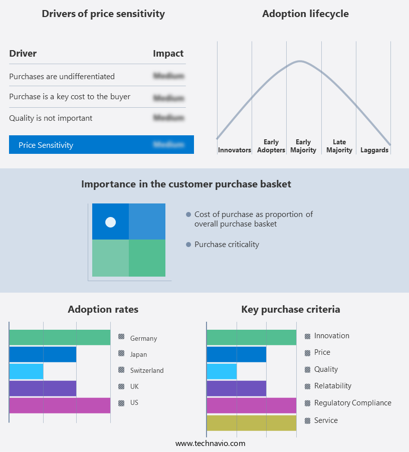
The focused ion beam market forecasting report includes the adoption lifecycle of the market, covering from the innovator's stage to the laggard's stage. It focuses on adoption rates in different regions based on penetration. Furthermore, the focused ion beam market report also includes key purchase criteria and drivers of price sensitivity to help companies evaluate and develop their market growth analysis strategies.
Customer Landscape
Key Companies & Market Insights
Companies are implementing various strategies, such as strategic alliances, focused ion beam market forecast, partnerships, mergers and acquisitions, geographical expansion, and product/service launches, to enhance their presence in the industry.
A and D HOLON Holdings Co. Ltd. - The Focused Ion Beam (FIB) market showcases the integration of advanced technologies, enabling high-resolution serial sectioning for intricate 3D structural analysis. Ideal for Transmission Electron Microscopy (TEM) and Three-Dimensional Atomic Probe (3DAP) analyses, this FIB solution, under the brand name AND, delivers optimized performance.
The industry research and growth report includes detailed analyses of the competitive landscape of the market and information about key companies, including:
- A and D HOLON Holdings Co. Ltd.
- Applied Beams LLC
- AZoM.com Ltd.
- Carl Zeiss AG
- Digital Surf SARL
- EAG Laboratories
- Fibics Inc.
- Fit4Nano
- Hitachi High Tech Corp.
- Honeywell International Inc.
- HORIBA Ltd.
- JEOL Ltd
- NANO-MASTER Inc.
- Nanosurf AG
- Raith GmbH
- TESCAN GROUP
- Thermo Fisher Scientific Inc.
- Veeco Instruments Inc.
- Waters Corp.
- zeroK NanoTech
Qualitative and quantitative analysis of companies has been conducted to help clients understand the wider business environment as well as the strengths and weaknesses of key industry players. Data is qualitatively analyzed to categorize companies as pure play, category-focused, industry-focused, and diversified; it is quantitatively analyzed to categorize companies as dominant, leading, strong, tentative, and weak.
Research Analyst Overview
The focused ion beam (FIB) market encompasses a diverse range of applications in various fields, including semiconductor manufacturing, physics, chemistry, engineering, biomaterials, nanomaterials, organic materials, smart materials, and more. FIB systems utilize a high-energy ion beam to precisely modify and manipulate materials at the nanoscale. In the realm of semiconductor manufacturing, FIB plays a crucial role in the creation and modification of integrated circuits (ICs). FIB is employed for various applications such as circuit editing, layout verification, mask repair, and site-specific analysis. These capabilities enable IC manufacturers to address defects, improve performance, and enhance the overall functionality of their products.
FIB technology is also extensively used in material science and life science research. In material science, FIB is applied for the manipulation of thin films, solid state nanopores, and the deposition of various materials. In life science, FIB is utilized for the preparation of samples for electron microscopy, 3D visualization, and nanoscale machining. The application of FIB in biotechnology and nanoscale machining offers significant potential for the development of advanced technologies. For instance, FIB is used to create porous materials, including mesopores and macropores, which can be employed in various applications such as environmental sensing, energy storage, and drug delivery systems.
FIB systems are also used in the field of electronics and semiconductor manufacturing for cryogenic and dual beam applications. These systems enable the analysis and modification of materials at low temperatures, which is essential for certain applications, such as the study of superconductors. Dual beam FIB systems combine the capabilities of both a focused ion beam and a scanning electron microscope, offering enhanced functionality for material analysis and imaging. FIB technology is also used in the field of 3D reconstruction, enabling the creation of precise 3D models of complex structures. This capability is particularly valuable in the field of biology, where it can be used to study cell morphology and the structure of biological samples.
FIB systems are essential tools in the field of nanotechnology, offering the ability to manipulate materials at the nanoscale with high precision. The use of gallium ions in FIB systems is particularly noteworthy due to their unique properties, which enable the precise modification of various materials. FIB technology is also used in the field of robotics and automation, enhancing the capabilities of these systems by enabling precise material manipulation and modification. This is particularly valuable in the field of IC repair, where FIB systems can be used to repair electrical connections and manipulate conductive materials. The development of FIB systems continues to advance, with ongoing research focusing on improving resolution, beam energies, and the integration of various capabilities, such as transmission electron microscopy and plasma ion sources.
These advancements are expected to expand the range of applications for FIB systems and drive growth in the market. In conclusion, the market is a dynamic and diverse field, encompassing a wide range of applications in various industries. FIB technology offers unique capabilities for material manipulation and analysis at the nanoscale, making it an essential tool for researchers and manufacturers in fields such as semiconductor manufacturing, material science, life science, and nanotechnology. The ongoing development of FIB systems is expected to drive growth in the market and expand the range of applications for this versatile technology.
|
Market Scope |
|
|
Report Coverage |
Details |
|
Page number |
150 |
|
Base year |
2023 |
|
Historic period |
2018-2022 |
|
Forecast period |
2024-2028 |
|
Growth momentum & CAGR |
Accelerate at a CAGR of 10.03% |
|
Market growth 2024-2028 |
USD 677.6 million |
|
Market structure |
Fragmented |
|
YoY growth 2023-2024(%) |
8.88 |
|
Key countries |
US, Japan, UK, Germany, and Switzerland |
|
Competitive landscape |
Leading Companies, Market Positioning of Companies, Competitive Strategies, and Industry Risks |
What are the Key Data Covered in this Focused Ion Beam Market Research and Growth Report?
- CAGR of the Focused Ion Beam industry during the forecast period
- Detailed information on factors that will drive the growth and forecasting between 2024 and 2028
- Precise estimation of the size of the market and its contribution of the industry in focus to the parent market
- Accurate predictions about upcoming growth and trends and changes in consumer behaviour
- Growth of the market across North America, Europe, APAC, Middle East and Africa, and South America
- Thorough analysis of the market's competitive landscape and detailed information about companies
- Comprehensive analysis of factors that will challenge the focused ion beam market growth of industry companies
We can help! Our analysts can customize this focused ion beam market research report to meet your requirements.
 RIA -
RIA -