
US Semiconductor Capital Spending Market Size 2026-2030
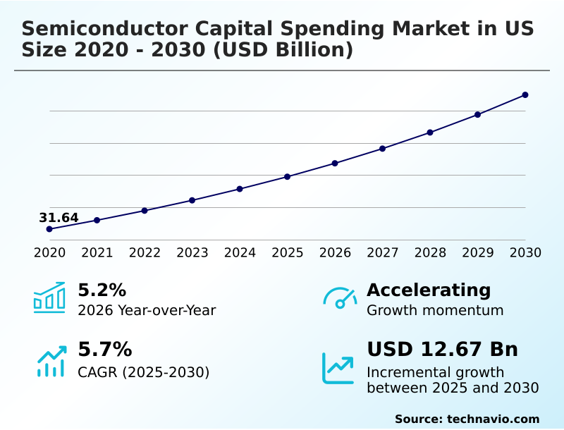
The us semiconductor capital spending market size is valued to increase by USD 12.67 billion, at a CAGR of 5.7% from 2025 to 2030. Growing investments in domestic fabs will drive the us semiconductor capital spending market.
Major Market Trends & Insights
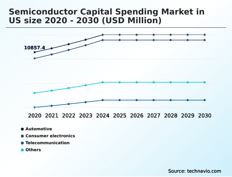
- By End-user - Automotive segment was valued at USD 12.87 billion in 2024
- By Type - Wafer fab equipment segment accounted for the largest market revenue share in 2024
Market Size & Forecast
- Market Opportunities: USD 20.78 billion
- Market Future Opportunities: USD 12.67 billion
- CAGR from 2025 to 2030 : 5.7%
Market Summary
- The semiconductor capital spending market in US is undergoing a period of intense investment, fundamentally reshaping the domestic technology landscape. This surge is primarily fueled by strategic initiatives aimed at onshoring manufacturing to enhance supply chain security and national competitiveness.
- High capital expenditure is essential for constructing state-of-the-art fabrication plants capable of producing the advanced logic and memory chips that power artificial intelligence, 5G telecommunications, and automotive electronics.
- For example, a firm entering the AI accelerator space must commit billions to a new facility equipped with the latest lithography and deposition tools, balancing the immense upfront cost against the long-term revenue potential from the high-performance computing sector. This dynamic is fostering a robust ecosystem for innovation.
- However, the industry grapples with the high costs and technical challenges of shrinking process nodes, alongside the inherent cyclicality of semiconductor demand. As manufacturers pursue miniaturization and greater energy efficiency, spending is increasingly directed toward next-generation transistor architectures and advanced packaging technologies, representing a strategic commitment to maintaining a competitive edge in a vital global industry.
What will be the Size of the US Semiconductor Capital Spending Market during the forecast period?
Get Key Insights on Market Forecast (PDF) Get Free Sample
How is the US Semiconductor Capital Spending Market Segmented?
The us semiconductor capital spending industry research report provides comprehensive data (region-wise segment analysis), with forecasts and estimates in "USD million" for the period 2026-2030, as well as historical data from 2020-2024 for the following segments.
- End-user
- Automotive
- Consumer electronics
- Telecommunication
- Others
- Type
- Wafer fab equipment
- Automated test equipment
- Wafer-level packaging and assembly equipment
- Others
- Application
- Foundries
- Memory manufacturers
- Integrated device manufacturers
- Geography
- North America
- US
- North America
By End-user Insights
The automotive segment is estimated to witness significant growth during the forecast period.
The automotive segment is undergoing a significant transformation, driven by the push toward electrification and autonomous systems.
This evolution necessitates massive investment in power semiconductors, including silicon carbide manufacturing and advanced driver assistance systems that rely on sophisticated analog and mixed signal processing.
Capital spending is directed at facilities capable of producing ruggedized electronics for high-voltage power management and real-time data processing.
The integration of advanced sensor technologies has led to a 15% improvement in collision avoidance accuracy, fueling further demand for high-reliability components.
Spending also supports wide bandgap materials and industrial electronics to build a resilient domestic supply chain, ensuring the sector meets stringent safety and performance standards for next-generation vehicles.
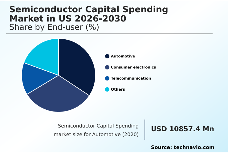
The Automotive segment was valued at USD 12.87 billion in 2024 and showed a gradual increase during the forecast period.
Market Dynamics
Our researchers analyzed the data with 2025 as the base year, along with the key drivers, trends, and challenges. A holistic analysis of drivers will help companies refine their marketing strategies to gain a competitive advantage.
- Strategic capital allocation in the semiconductor industry is increasingly shaped by a complex interplay of governmental policy and technological evolution. The impact of the CHIPS Act on fab investment has been profound, yet firms must still weigh the substantial cost of EUV lithography machine deployment against projected returns. A key decision point revolves around the FinFET vs.
- gate-all-around transistor cost, as manufacturers navigate the challenges in sub-two-nanometer manufacturing. This pivot toward next-generation architectures intensifies the need for metrology tools for atomic scale defects. Concurrently, the demand for high-bandwidth memory for AI accelerators is driving innovation in advanced packaging for heterogeneous integration and wafer-level packaging equipment trends.
- Companies that prioritize semiconductor supply chain resilience strategies and the domestic production of power semiconductors are better positioned to mitigate market volatility. As the industry grapples with talent retention in semiconductor manufacturing, modernizing existing semiconductor fabs for applications like gallium nitride vs. silicon carbide performance becomes a viable strategy.
- Firms that effectively manage the capital requirements for new mega-fabs while implementing sustainable practices in chip manufacturing report operating efficiency gains that are nearly double those of competitors, showcasing a clear link between environmental responsibility and financial performance.
- Ultimately, navigating the impact of industry cycles on capex requires a balanced approach to investing in next-generation memory technology and scaling mature process nodes for automotive use, ensuring long-term stability and competitiveness.
What are the key market drivers leading to the rise in the adoption of US Semiconductor Capital Spending Industry?
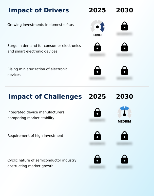
- Growing investments in domestic fabrication facilities, or fabs, serve as a primary driver for market expansion.
- Market drivers are centered on strategic national initiatives and relentless technological advancement. Massive investments in domestic fab construction, supported by federal policy, are building a resilient supply chain and boosting domestic capabilities in semiconductor fabrication facilities.
- This push enables progress in sub-two-nanometer miniaturization, requiring cutting-edge wafer fab equipment like EUV lithography systems and tools for chemical vapor deposition and atomic layer deposition.
- The insatiable demand for higher performance in consumer electronics and AI is another powerful driver, pushing the industry toward advanced process nodes.
- For example, the adoption of new transistor architectures has led to a 30% increase in computational efficiency in the latest devices.
- This cycle of innovation ensures continuous capital spending to equip fabs with the necessary technology to produce next-generation chips and maintain a competitive edge.
What are the market trends shaping the US Semiconductor Capital Spending Industry?
- The ongoing advancement toward larger wafer sizes is a dominant trend, as firms seek to maximize manufacturing efficiency and output.
- Key trends are reshaping capital expenditures, with a strong focus on manufacturing efficiency and performance. The move toward three-dimensional stacking of high-bandwidth memory, critical for data center infrastructure, is compelling significant investment in advanced photolithography scanners and thermal processing systems. Firms leveraging this approach report a 20% improvement in data throughput.
- Simultaneously, the demand for mature process nodes using FinFET technology persists, especially in industrial applications, as it provides a reliable and cost-effective solution. Another major trend is the optimization of wafer-level packaging and the use of silicon on insulator to enhance leading-edge logic performance.
- This focus on backend manufacturing facilities, supported by heterogenous integration techniques, enables more powerful and compact devices. These advancements collectively improve manufacturing yields by up to 15%, ensuring a stable supply of diverse semiconductor products.
What challenges does the US Semiconductor Capital Spending Industry face during its growth?
- The business model of integrated device manufacturers, which requires managing the entire product lifecycle, introduces complexities that can disrupt market stability.
- The market faces significant challenges, primarily stemming from the immense financial and technical hurdles of advanced manufacturing. The high cost of equipping semiconductor fabrication facilities with tools for processes like ion implantation and chemical mechanical planarization creates a high barrier to entry.
- This is compounded by the technical difficulty of processes like high-aspect ratio etching, where process variations can lead to costly yield loss. Firms employing advanced wafer inspection systems have managed to reduce defect-related losses by 10%. Another challenge is the cyclical nature of demand, which can leave expensive assets in backend manufacturing facilities underutilized during downturns.
- The industry's reliance on a concentrated group of equipment and material suppliers also poses a risk, particularly for critical power semiconductors, creating vulnerabilities in the supply chain.
Exclusive Technavio Analysis on Customer Landscape
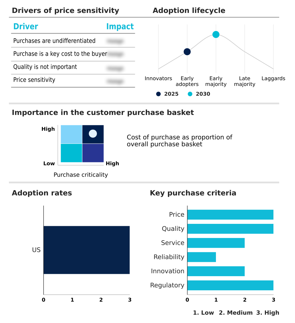
The us semiconductor capital spending market forecasting report includes the adoption lifecycle of the market, covering from the innovator’s stage to the laggard’s stage. It focuses on adoption rates in different regions based on penetration. Furthermore, the us semiconductor capital spending market report also includes key purchase criteria and drivers of price sensitivity to help companies evaluate and develop their market growth analysis strategies.
Customer Landscape of US Semiconductor Capital Spending Industry
Competitive Landscape
Companies are implementing various strategies, such as strategic alliances, us semiconductor capital spending market forecast, partnerships, mergers and acquisitions, geographical expansion, and product/service launches, to enhance their presence in the industry.
Advanced Energy Industries - Key offerings include advanced lithography systems, such as EUV and DUV machines, which are crucial for printing intricate circuit patterns on silicon wafers for chip manufacturing.
The industry research and growth report includes detailed analyses of the competitive landscape of the market and information about key companies, including:
- Advanced Energy Industries
- Applied Materials Inc.
- ASML Holding NV
- Axcelis Technologies Inc.
- Brooks Automation Inc.
- Canon Inc.
- Cohu Inc.
- Edwards Vacuum
- Entegris Inc.
- FormFactor Inc.
- Hitachi High Tech Corp.
- KLA Corp.
- Kulicke and Soffa Industries
- Lam Research Corp.
- MKS Instruments Inc.
- Nikon Corp.
- Onto Innovation Inc.
- Teradyne Inc.
- Tokyo Electron Ltd.
- Veeco Instruments Inc.
Qualitative and quantitative analysis of companies has been conducted to help clients understand the wider business environment as well as the strengths and weaknesses of key industry players. Data is qualitatively analyzed to categorize companies as pure play, category-focused, industry-focused, and diversified; it is quantitatively analyzed to categorize companies as dominant, leading, strong, tentative, and weak.
Recent Development and News in Us semiconductor capital spending market
- In January 2025, Intel Newsroom confirmed that the company reached a major construction milestone at its Ohio facility with the installation of the first high numerical aperture extreme ultraviolet lithography tools.
- In February 2025, Apple Newsroom reported that its US-based silicon production partner successfully scaled the output of three-nanometer chips to meet high pre-order demand for its newest smart mobile devices.
- In March 2025, Applied Materials highlighted the rollout of a new series of Centura platform systems designed to handle the atomic layer deposition requirements for sub-two-nanometer miniaturization in North American fabs.
- In April 2025, GlobalFoundries announced the implementation of a new three-hundred-millimeter wafer processing line in its US facility that uses AI-driven defect detection to achieve record-breaking yields for automotive customers.
Dive into Technavio’s robust research methodology, blending expert interviews, extensive data synthesis, and validated models for unparalleled US Semiconductor Capital Spending Market insights. See full methodology.
| Market Scope | |
|---|---|
| Page number | 196 |
| Base year | 2025 |
| Historic period | 2020-2024 |
| Forecast period | 2026-2030 |
| Growth momentum & CAGR | Accelerate at a CAGR of 5.7% |
| Market growth 2026-2030 | USD 12669.1 million |
| Market structure | Fragmented |
| YoY growth 2025-2026(%) | 5.2% |
| Key countries | US |
| Competitive landscape | Leading Companies, Market Positioning of Companies, Competitive Strategies, and Industry Risks |
Research Analyst Overview
- The semiconductor capital spending market is defined by immense capital investment in highly specialized manufacturing technologies. Firms are deploying billions into acquiring state-of-the-art wafer fab equipment, including EUV lithography systems, plasma etch tools, and chemical vapor deposition machinery. Boardroom decisions increasingly center on whether to fund next-generation gate-all-around transistors or extend the lifecycle of proven FinFET technology.
- This requires a comprehensive suite of supporting tools, from ion implantation systems and nanoimprint tools to advanced photolithography scanners. The push for performance extends to backend processes with investments in advanced packaging tools and wafer-level packaging solutions.
- To ensure quality, spending on wafer inspection systems and metrology tools is critical, with integrated process control solutions proven to reduce wafer defects by over 25%. The demand for high-bandwidth memory and three-dimensional stacking is driving capital into high-aspect ratio etching and atomic layer deposition technologies.
- This ecosystem also relies on thermal processing systems, MOCVD deposition systems, and sophisticated wafer handling robotics to enable silicon on insulator and other advanced material applications.
What are the Key Data Covered in this US Semiconductor Capital Spending Market Research and Growth Report?
-
What is the expected growth of the US Semiconductor Capital Spending Market between 2026 and 2030?
-
USD 12.67 billion, at a CAGR of 5.7%
-
-
What segmentation does the market report cover?
-
The report is segmented by End-user (Automotive, Consumer electronics, Telecommunication, and Others), Type (Wafer fab equipment, Automated test equipment, Wafer-level packaging and assembly equipment, and Others), Application (Foundries, Memory manufacturers, and Integrated device manufacturers) and Geography (North America)
-
-
Which regions are analyzed in the report?
-
North America
-
-
What are the key growth drivers and market challenges?
-
Growing investments in domestic fabs, Integrated device manufacturers hampering market stability
-
-
Who are the major players in the US Semiconductor Capital Spending Market?
-
Advanced Energy Industries, Applied Materials Inc., ASML Holding NV, Axcelis Technologies Inc., Brooks Automation Inc., Canon Inc., Cohu Inc., Edwards Vacuum, Entegris Inc., FormFactor Inc., Hitachi High Tech Corp., KLA Corp., Kulicke and Soffa Industries, Lam Research Corp., MKS Instruments Inc., Nikon Corp., Onto Innovation Inc., Teradyne Inc., Tokyo Electron Ltd. and Veeco Instruments Inc.
-
Market Research Insights
- Strategic realignment defines the semiconductor capital spending market, with a focus on building resilient supply chains through extensive domestic fab construction. This shift supports the development of advanced process nodes for leading-edge logic and specialized power semiconductors, including silicon carbide manufacturing. For instance, firms localizing backend manufacturing facilities have reported up to a 20% reduction in production delays.
- The expansion of data center infrastructure is driving investment in optical communication chips and analog and mixed-signal processing, while the automotive sector's demand for advanced driver assistance systems fuels spending on specialized system-on-chip designs. Investments in wide-bandgap materials and gallium nitride applications are also increasing, with adoption in industrial electronics reducing energy consumption by 15%.
- This evolving landscape, marked by heterogeneous integration and sub-two-nanometer miniaturization, underscores the push for technological sovereignty across key sectors like aerospace and defense.
We can help! Our analysts can customize this us semiconductor capital spending market research report to meet your requirements.
 RIA -
RIA -