
Semiconductor Wafer Polishing and Grinding Equipment Market Size 2024-2028
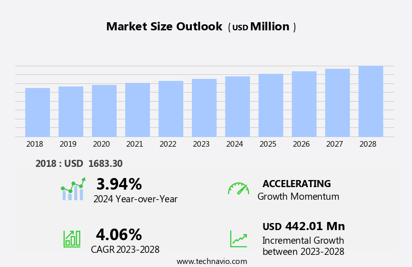
The semiconductor wafer polishing and grinding equipment market size is forecast to increase by USD 442.01 million at a CAGR of 4.06% between 2023 and 2028.
What will be the Size of the Semiconductor Wafer Polishing and Grinding Equipment Market During the Forecast Period?
How is this Semiconductor Wafer Polishing and Grinding Equipment Industry segmented and which is the largest segment?
The semiconductor wafer polishing and grinding equipment industry research report provides comprehensive data (region-wise segment analysis), with forecasts and estimates in "USD million" for the period 2024-2028, as well as historical data from 2018-2022 for the following segments.
- Application
- 300 mm
- 200 mm
- Less than 200 mm
- End-user
- Foundries
- IDM
- Memory manufacturers
- Geography
- APAC
- China
- Japan
- South Korea
- North America
- US
- Europe
- South America
- Middle East and Africa
- APAC
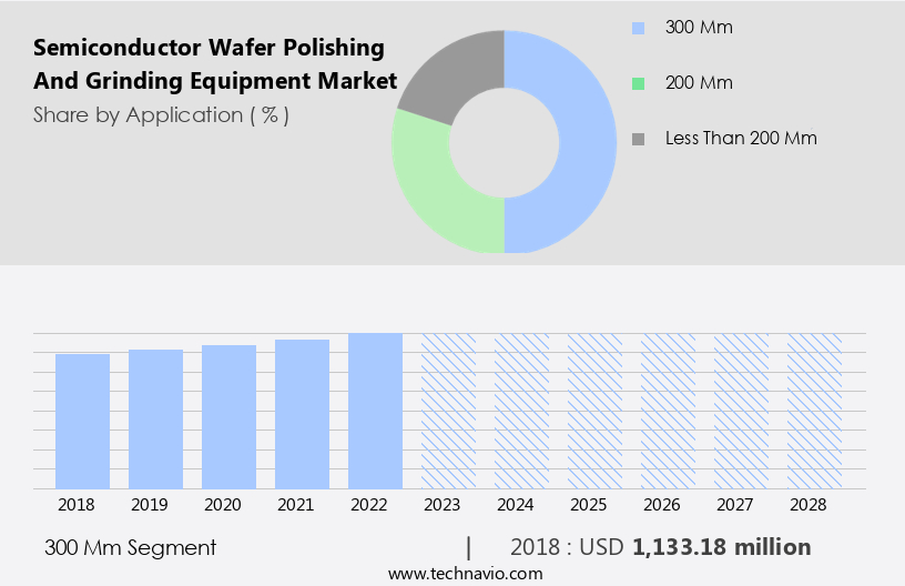
By Application Insights
The 300 mm segment is estimated to witness significant growth during the forecast period. The market is driven by the increasing demand for ultra-precise wafers In the semiconductor industry. Innovations in semiconductor wafer research, such as wafer bonding, etching, simulation, and design, require advanced grinding and polishing techniques to achieve high surface quality. Automated wafer handling and metrology are essential for maintaining semiconductor yields and ensuring performance standards. Semiconductor manufacturing equipment companies invest heavily in high-precision polishing and grinding technologies to meet the demands of next-generation wafer fabrication. These include ultra-thin wafers for applications in 5G technology, data centers, renewable energy, nanotechnology, and semiconductor device fabrication. The market trends include waste reduction, energy-efficient production, and eco-friendly manufacturing.
Major semiconductor manufacturers, such as Samsung, Micron Technology, and SK Hynix, utilize large-scale 300 mm wafers for memory IC production. Foundries like Taiwan Semiconductor Manufacturing Company, Globalfoundries, United Microelectronics, and SMIC also develop ICs on 300 mm wafers. The bulk production and financial resources required to expand 300 mm fabs fuel the demand for wafers and grinding equipment. Semiconductor wafer inspection, cleaning, and packaging are crucial steps In the semiconductor manufacturing process. Grinding processes and wafer thinning are essential for achieving the required surface quality for various semiconductor applications, including power electronics, automotive electronics, artificial intelligence applications, and high-performance computing.
The semiconductor wafer market is expected to grow significantly due to the increasing demand for advanced semiconductor technologies and applications.
Get a glance at the market report of various segments Request Free Sample
The 300 mm segment was valued at USD 1133.18 million in 2018 and showed a gradual increase during the forecast period.
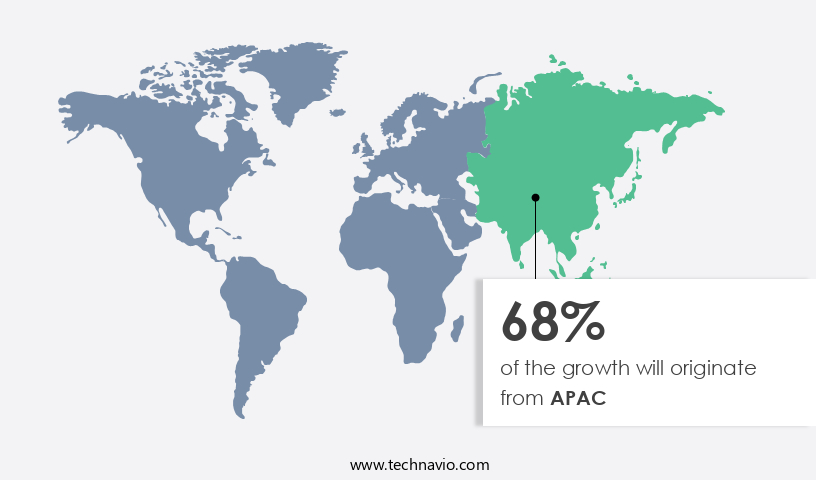
Regional Analysis
APAC is estimated to contribute 68% to the growth of the global market during the forecast period. Technavio’s analysts have elaborately explained the regional trends and drivers that shape the market during the forecast period.
For more insights on the market size of various regions, Request Free Sample
In the APAC region, the presence of leading semiconductor foundries, including TSMC, Samsung, and SMIC, drives the demand for semiconductor wafer polishing and grinding equipment. Key countries such as Taiwan, South Korea, Japan, and China, which house major semiconductor device manufacturers, significantly contribute to the market's growth. The consumer electronics and mobile devices sector, dominated by companies like Samsung, Sony, LG, Toshiba, and Panasonic, fuels the demand for semiconductor wafers in APAC. The increasing requirement for miniaturized Integrated Circuits (ICs) in industries such as consumer, healthcare, optical, and others, is attributed to advancements in wired and wireless technologies, the growing implementation of Internet of Things (IoT), increasing automation, and investment in Human-Machine Interface (HMI) technologies.
The semiconductor wafer market trends include the demand for ultra-precise wafers, high-performance semiconductor manufacturing equipment, and eco-friendly wafer manufacturing. The semiconductor wafer innovation, research, and development focus on wafer bonding, etching, simulation, cleaning, grinding, metrology, packaging, inspection, and testing. The semiconductor industry's future lies in next-generation wafer fabrication, sustainable manufacturing, energy-efficient production, and green semiconductor manufacturing. The semiconductor wafer applications span across 5G technology, renewable energy, data centers, nanotechnology, semiconductor device fabrication, integrated circuit fabrication, deep learning, power electronics, ultra-thin wafers, connected vehicles, machine learning algorithms, chip manufacturing, microelectronics, wafer surface metrology, three dimensional stacking, smart mobility, edge computing, artificial intelligence applications, future of electronics, automotive electronics, natural language processing, high-performance computing, and energy storage.
Market Dynamics
Our researchers analyzed the data with 2023 as the base year, along with the key drivers, trends, and challenges. A holistic analysis of drivers will help companies refine their marketing strategies to gain a competitive advantage.
What are the key market drivers leading to the rise In the adoption of Semiconductor Wafer Polishing and Grinding Equipment Industry?
- Emergence of miniaturized semiconductor components is the key driver of the market.In the evolving semiconductor landscape, the focus on miniaturization is a significant trend. The semiconductor industry is witnessing an increased demand for compact electronic devices, which necessitates the production of smaller, high-performance components. Wafer polishing and grinding equipment play a pivotal role in transferring intricate IC designs from photomasks to ultra-precise silicon wafers. This process is crucial for semiconductor wafer etching, bonding, and packaging, ensuring the production of high-quality, high-yield wafers. Semiconductor wafer innovation and research continue to drive advancements in wafer polishing and grinding technology. Automated wafer handling, high-precision polishing, and eco-friendly manufacturing processes are becoming increasingly important.
Wafer cleaning, defect detection, and metrology are essential for maintaining wafer surface quality. The semiconductor wafer market is witnessing growth due to the increasing demand for 5G technology, renewable energy, data centers, and nanotechnology applications. Performance standards, energy efficiency, and waste reduction are key considerations for semiconductor manufacturing equipment. Semiconductor wafer trends include the adoption of three-dimensional stacking, machine learning algorithms, and artificial intelligence applications. These advancements require next-generation grinding and polishing techniques for producing ultra-thin wafers and improving chip manufacturing efficiency. Semiconductor wafer technology is also expanding into new areas such as power electronics, connected vehicles, and smart mobility.
Wafer thinning, surface metrology, and automated wafer polishing are essential for producing high-performance components In these emerging markets. In summary, the market is a dynamic and evolving sector that plays a vital role In the production of advanced semiconductor components. The focus on miniaturization, performance, and eco-friendliness is driving innovation and growth in this market.
What are the market trends shaping the Semiconductor Wafer Polishing and Grinding Equipment market?
- Increasing use of NEMS is the upcoming market trend.The semiconductor wafer innovation ecosystem encompasses various technologies and processes, including semiconductor wafer research, etching, simulation, bonding, cleaning, metrology, packaging, inspection, and grinding. Semiconductor wafer grinding equipment plays a crucial role in achieving ultra-precise wafers for high-performance applications. This market is driven by semiconductor manufacturing equipment trends, such as automated wafer handling, high-precision polishing, and eco-friendly wafer manufacturing. Semiconductor wafer technology advancements, including 5G technology, nanotechnology, and quantum computing, necessitate ultra-thin wafers and three-dimensional stacking. Wafer defect detection and waste reduction are critical performance standards in semiconductor manufacturing. Wafer grinding processes must ensure high-precision results to meet the demands of the semiconductor industry.
The semiconductor wafer market is expected to grow significantly due to applications in renewable energy, data centers, automotive electronics, and artificial intelligence. Next-generation wafer fabrication focuses on energy-efficient production and sustainable manufacturing. Semiconductor wafer equipment manufacturers must adhere to IEC standards and meet the evolving performance requirements of the industry. Semiconductor wafer trends include wafer surface quality improvements, high-performance computing, and chip manufacturing advancements. Machine learning algorithms and artificial intelligence applications are transforming semiconductor manufacturing processes. The future of electronics relies on continued innovation in semiconductor wafer technology, design, and manufacturing.
What challenges does the Semiconductor Wafer Polishing and Grinding Equipment Industry face during its growth?
- Increased gap between development time of semiconductor wafer polishing and grinding equipment and release to foundries is a key challenge affecting the industry growth.The semiconductor industry's growth trajectory drives the demand for advanced wafer polishing and grinding equipment. Semiconductor wafer innovation and research continue to push the boundaries of semiconductor wafer etching, bonding, and design. Consequently, semiconductor manufacturing equipment, including wafer polishing and grinding equipment, plays a pivotal role in achieving ultra-precise wafers and high semiconductor yields. Automated wafer handling, cleaning, inspection, and metrology are essential components of modern semiconductor wafer manufacturing. Wafer grinding equipment facilitates the removal of excess material, ensuring the required wafer thickness for semiconductor device fabrication. Wafer defect detection and reduction are crucial for maintaining high-performance standards In the semiconductor wafer market.
Semiconductor wafer trends include the adoption of eco-friendly wafer manufacturing, next-generation wafer fabrication, and energy-efficient wafer production. These trends are influenced by the increasing demand for 5G technology, renewable energy, data centers, and nanotechnology applications. Moreover, the integration of machine learning algorithms, artificial intelligence, and three-dimensional stacking in semiconductor manufacturing further enhances the importance of high-precision polishing and grinding processes. Semiconductor wafer testing, simulation, and packaging are essential steps In the semiconductor manufacturing process. The semiconductor wafer industry caters to various applications, including power electronics, automotive electronics, and integrated circuit fabrication. The future of electronics lies In the development of high-performance computing, quantum computing, and edge computing technologies.
As such, the demand for semiconductor wafer polishing and grinding equipment is expected to remain strong.
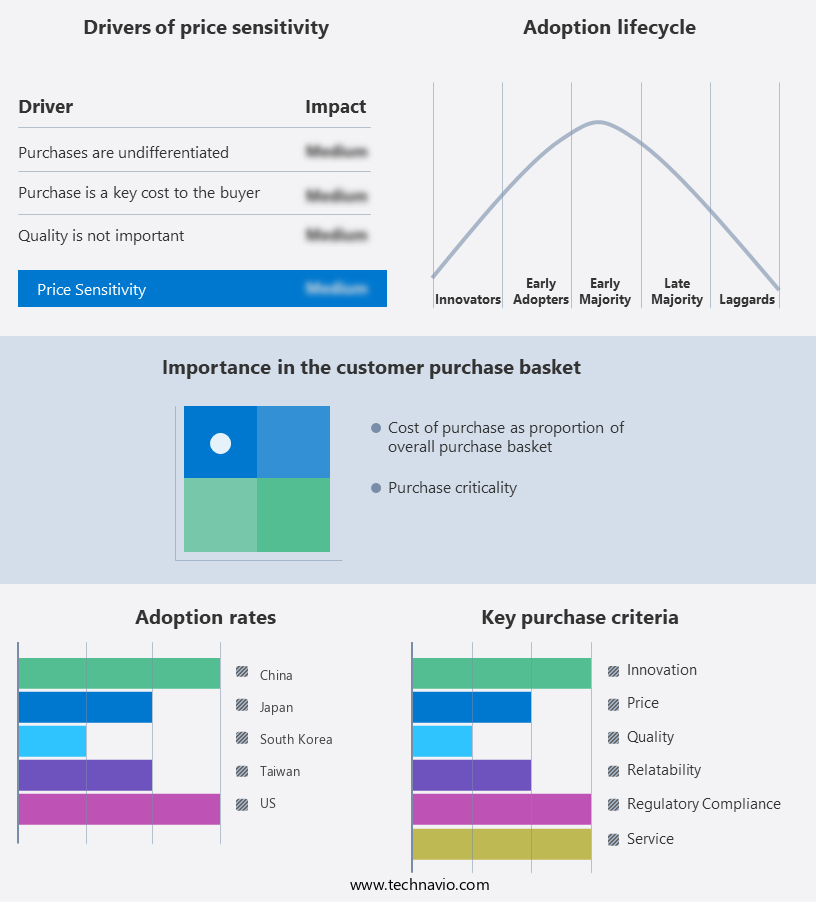
Exclusive Customer Landscape
The semiconductor wafer polishing and grinding equipment market forecasting report includes the adoption lifecycle of the market, covering from the innovator’s stage to the laggard’s stage. It focuses on adoption rates in different regions based on penetration. Furthermore, the semiconductor wafer polishing and grinding equipment market report also includes key purchase criteria and drivers of price sensitivity to help companies evaluate and develop their market growth analysis strategies.
Customer Landscape
Key Companies & Market Insights
Companies are implementing various strategies, such as strategic alliances, semiconductor wafer polishing and grinding equipment market forecast, partnerships, mergers and acquisitions, geographical expansion, and product/service launches, to enhance their presence In the industry.
ALLIED HIGH TECH PRODUCTS, INC - The market encompasses advanced technologies designed for the precise refinement of silicon wafers In the production of microelectronics. These systems employ various techniques, such as chemical mechanical polishing (CMP) and grinding, to create flat and smooth surfaces essential for semiconductor manufacturing. Market growth is driven by the increasing demand for smaller, faster, and more efficient electronic devices, necessitating continuous improvements in wafer processing technology. The equipment market caters to semiconductor manufacturers worldwide, enabling them to maintain high production standards and yield optimal results.
The industry research and growth report includes detailed analyses of the competitive landscape of the market and information about key companies, including:
- ALLIED HIGH TECH PRODUCTS, INC
- Amtech Systems Inc.
- Applied Materials Inc.
- ASM International NV
- Axus Technology
- DISCO Corp.
- G and N GmbH
- Gigamat Technologies Inc
- KLA Corp.
- Lapmaster Wolters
- Logitech Ltd.
- Okamoto Corp
- Revasum Inc.
- S Cubed
- S3 Alliance.
- Tokyo Electron Ltd.
- TOKYO SEIMITSU CO. LTD
- ULTRA TEC Manufacturing Inc.
- UNITED GRINDING North America, Inc.
- Ebara Corp.
Qualitative and quantitative analysis of companies has been conducted to help clients understand the wider business environment as well as the strengths and weaknesses of key industry players. Data is qualitatively analyzed to categorize companies as pure play, category-focused, industry-focused, and diversified; it is quantitatively analyzed to categorize companies as dominant, leading, strong, tentative, and weak.
Research Analyst Overview
The semiconductor wafer manufacturing industry continues to innovate and push the boundaries of technology, with a focus on producing ultra-precise wafers for various applications. Wafer polishing and grinding equipment play a crucial role in achieving the desired surface quality and dimensions for these advanced semiconductor components. Semiconductor wafer research and development efforts are dedicated to enhancing wafer fabrication processes, such as wafer bonding, etching, and simulation. Automated wafer handling systems have become essential in ensuring consistent and efficient production. These advancements aim to improve semiconductor yields and reduce waste, making manufacturing processes more sustainable. The semiconductor wafer market is driven by the increasing demand for high-performance components in various industries, including telecommunications, renewable energy, data centers, and automotive electronics.
Performance standards and IEC regulations are essential in ensuring the quality and safety of these components. Semiconductor wafer trends include the adoption of next-generation wafer fabrication techniques, such as eco-friendly manufacturing, energy-efficient production, and green semiconductor manufacturing. These approaches aim to minimize environmental impact and reduce the carbon footprint of semiconductor manufacturing. Advancements in wafer grinding equipment and processes have led to high-precision polishing and grinding capabilities. These technologies enable the production of ultra-thin wafers, which are essential for the development of advanced semiconductor devices and integrated circuits. Semiconductor wafer cleaning and inspection processes are critical in ensuring the quality of the final product.
Wafer defect detection and metrology techniques are continually evolving to identify and address defects at the earliest stages of production. The integration of machine learning algorithms and artificial intelligence applications in semiconductor manufacturing is transforming the industry. These technologies enable predictive maintenance, optimized production, and improved quality control. Semiconductor wafer technology continues to advance, with a focus on three-dimensional stacking, smart mobility, edge computing, and high-performance computing. These technologies are essential in powering the next generation of electronics, including 5G technology, quantum computing, and artificial intelligence. In conclusion, the semiconductor wafer manufacturing industry is undergoing significant changes, driven by the need for high-performance components and sustainable manufacturing processes.
Wafer polishing and grinding equipment play a crucial role in achieving the desired surface quality and dimensions for these advanced semiconductor components. The integration of automation, eco-friendly manufacturing, and advanced technologies is transforming the industry and setting the stage for the future of electronics.
|
Market Scope |
|
|
Report Coverage |
Details |
|
Page number |
172 |
|
Base year |
2023 |
|
Historic period |
2018-2022 |
|
Forecast period |
2024-2028 |
|
Growth momentum & CAGR |
Accelerate at a CAGR of 4.06% |
|
Market growth 2024-2028 |
USD 442.01 million |
|
Market structure |
Fragmented |
|
YoY growth 2023-2024(%) |
3.94 |
|
Key countries |
US, South Korea, Taiwan, China, and Japan |
|
Competitive landscape |
Leading Companies, Market Positioning of Companies, Competitive Strategies, and Industry Risks |
What are the Key Data Covered in this Semiconductor Wafer Polishing and Grinding Equipment Market Research and Growth Report?
- CAGR of the Semiconductor Wafer Polishing and Grinding Equipment industry during the forecast period
- Detailed information on factors that will drive the growth and forecasting between 2024 and 2028
- Precise estimation of the size of the market and its contribution of the industry in focus to the parent market
- Accurate predictions about upcoming growth and trends and changes in consumer behaviour
- Growth of the market across APAC, North America, Europe, South America, and Middle East and Africa
- Thorough analysis of the market’s competitive landscape and detailed information about companies
- Comprehensive analysis of factors that will challenge the semiconductor wafer polishing and grinding equipment market growth of industry companies
We can help! Our analysts can customize this semiconductor wafer polishing and grinding equipment market research report to meet your requirements.
 RIA -
RIA -