Wafer-level Manufacturing Equipment Market Size 2026-2030
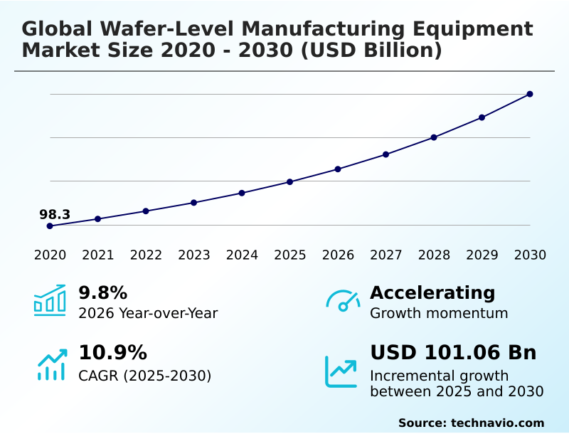
The wafer-level manufacturing equipment market size is valued to increase by USD 101.06 billion, at a CAGR of 10.9% from 2025 to 2030. Exponential growth in high-performance computing and data center infrastructure will drive the wafer-level manufacturing equipment market.
Major Market Trends & Insights
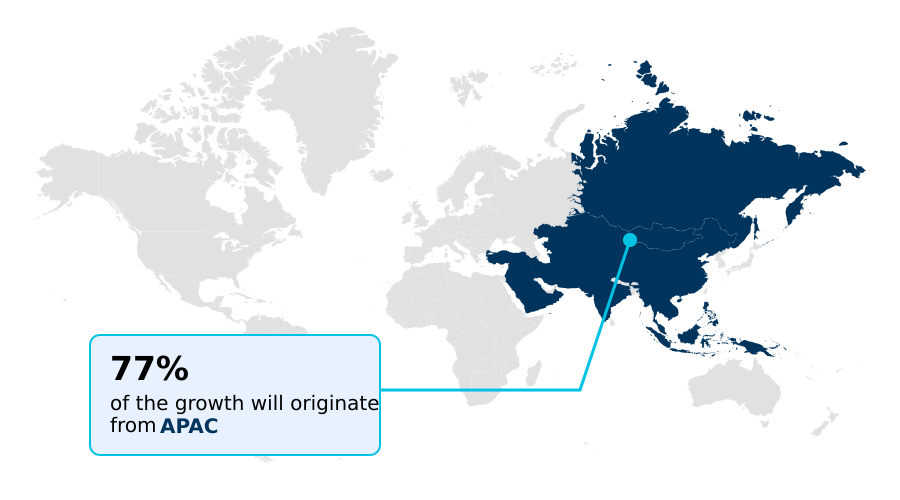
- APAC dominated the market and accounted for a 77.2% growth during the forecast period.
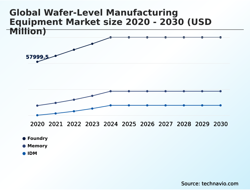
- By End-user - Foundry segment was valued at USD 77.00 billion in 2024
- By Product - Wafer fab equipment segment accounted for the largest market revenue share in 2024
Market Size & Forecast
- Market Opportunities: USD 151.76 billion
- Market Future Opportunities: USD 101.06 billion
- CAGR from 2025 to 2030 : 10.9%
Market Summary
- The wafer-level manufacturing equipment market is characterized by a dynamic interplay of technological advancement and escalating end-user demand. The industry is propelled by the need for smaller, more powerful semiconductors for applications in AI, 5G, and high-performance computing, which requires constant innovation in equipment for processes like EUV lithography and atomic layer deposition.
- A primary trend is the adoption of advanced packaging technology, including heterogeneous integration, to overcome the limitations of traditional scaling. A fabless design house, for instance, must secure capacity at foundries with state-of-the-art process control solutions to ensure their complex chiplet-based designs meet performance targets and time-to-market schedules.
- However, the market faces challenges from the extreme capital cost of next-generation equipment and the technical complexities of thin-wafer handling. The industry's trajectory hinges on balancing these high investment costs with the manufacturing efficiencies gained from advanced equipment that enables superior yield optimization.
What will be the Size of the Wafer-level Manufacturing Equipment Market during the forecast period?
Get Key Insights on Market Forecast (PDF) Get Free Sample
How is the Wafer-level Manufacturing Equipment Market Segmented?
The wafer-level manufacturing equipment industry research report provides comprehensive data (region-wise segment analysis), with forecasts and estimates in "USD million" for the period 2026-2030, as well as historical data from 2020-2024 for the following segments.
- End-user
- Foundry
- Memory
- IDM
- Product
- Wafer fab equipment
- Wafer level packaging
- Technology
- Photolithography equipment
- Etching equipment
- Component
- Equipment hardware
- Software solutions
- Geography
- APAC
- China
- Japan
- India
- North America
- US
- Canada
- Mexico
- Europe
- Germany
- UK
- France
- South America
- Brazil
- Argentina
- Middle East and Africa
- Saudi Arabia
- UAE
- South Africa
- Rest of World (ROW)
- APAC
By End-user Insights
The foundry segment is estimated to witness significant growth during the forecast period.
The foundry segment is pivotal to semiconductor fabrication, providing contract integrated circuit manufacturing for a diverse fabless client base. This model requires continuous investment in cutting-edge wafer-level equipment to support varied designs, including emerging chiplet architectures.
The relentless need for precision necessitates robust process control solutions to manage complex workflows involving deposition, bonding, and testing.
Effective implementation of these capabilities is critical for superior yield optimization, with some operations reporting a defect reduction of more than 10% on new process ramps.
This underscores their crucial role in the electronics supply chain and the demand for tools like those for chemical mechanical planarization (cmp).
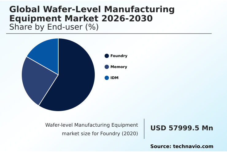
The Foundry segment was valued at USD 77.00 billion in 2024 and showed a gradual increase during the forecast period.
Regional Analysis
APAC is estimated to contribute 77.2% to the growth of the global market during the forecast period.Technavio’s analysts have elaborately explained the regional trends and drivers that shape the market during the forecast period.
See How Wafer-level Manufacturing Equipment Market Demand is Rising in APAC Get Free Sample
The geographic landscape is dominated by APAC, which represents over 77% of the market opportunity, driven by its massive concentration of semiconductor fabrication facilities.
This region is a primary consumer of equipment for creating through-silicon vias (tsvs) and implementing atomic layer deposition (ald) for advanced memory. North America is revitalizing its domestic manufacturing, focusing on leading-edge logic for its strong IDM base.
Europe leverages its strength in automotive and industrial sectors, specializing in wafer-level optics (wlo). Across all regions, the adoption of advanced software solutions is critical.
Integrating tools for ion implantation, laser annealing, wet processing systems, and wafer bonding and debonding with AI-driven analytics has improved process stability, reducing wafer-to-wafer variability by as much as 15% in advanced fabs.
Market Dynamics
Our researchers analyzed the data with 2025 as the base year, along with the key drivers, trends, and challenges. A holistic analysis of drivers will help companies refine their marketing strategies to gain a competitive advantage.
- The wafer-level manufacturing equipment market is evolving rapidly to address increasingly complex semiconductor designs. Strategic decisions now revolve around the role of AI in semiconductor yield optimization, which has become crucial for mitigating the prohibitive cost of advanced photolithography systems. The technical challenges in thin-wafer handling and processing for high-volume manufacturing require innovative solutions, especially for advanced packaging.
- This includes specialized equipment for fan-out wafer level packaging and redistribution layer patterning techniques. The shift to disaggregated designs is driving demand for hybrid bonding equipment for chiplet integration and through-silicon via formation process tools. In memory manufacturing, specific etching equipment for 3d nand manufacturing and processes like atomic layer deposition in memory fabrication are key investment areas.
- The move to new architectures also requires advanced metrology systems for gate-all-around transistors and inspection systems for 3d-stacked architectures, which are more complex than their predecessors by a factor of two. For specialized applications, demand for drie tools for mems device fabrication and equipment for sic and gan wafer processing is growing.
- Looking forward, advances in wafer bonding and debonding technology and improving euv lithography source power and uptime are top priorities. The market is also seeing new applications for plasma therm systems for nanoscale processing and wafer-level optics manufacturing equipment.
- However, the impact of geopolitics on semiconductor equipment supply and the need for robust software solutions for wafer fab automation introduce significant operational risks that companies must navigate.
What are the key market drivers leading to the rise in the adoption of Wafer-level Manufacturing Equipment Industry?
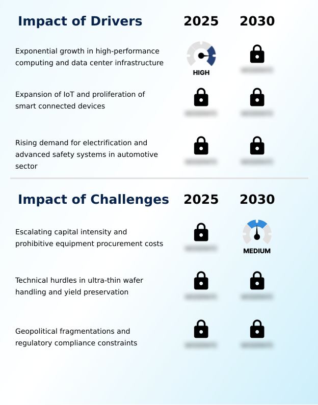
- The exponential growth in high-performance computing and the expansion of data center infrastructure are key drivers for the market.
- Growth in data centers and automotive electronics is a primary driver. Demand from memory and idm sectors for higher-density chips necessitates advanced wafer fab equipment.
- The proliferation of microelectromechanical systems (mems) for automotive sensors, fabricated using techniques like deep reactive-ion etching (drie) and high-aspect-ratio etching, has increased semiconductor content per vehicle by over 25%.
- This requires specialized tools, including those for hybrid bonding and metal-organic chemical vapor deposition (mocvd).
- Furthermore, equipment like mask aligners and sputtering systems are crucial for producing the power semiconductors and sensors that underpin vehicle electrification and autonomy, creating a sustained demand cycle.
What are the market trends shaping the Wafer-level Manufacturing Equipment Industry?
- The proliferation of heterogeneous integration and chiplet-based architectures represents a key upcoming trend. This shift is reshaping semiconductor design and manufacturing principles.
- The shift toward heterogeneous integration and advanced packaging technology is fundamentally reshaping the market. As conventional scaling faces limitations, 3d-ic integration and fan-out wafer level packaging (fowlp) have become essential for creating high-performance devices. This trend drives significant investment in equipment hardware capable of sub-micron alignment and patterning complex redistribution layers (rdls).
- The evolution toward panel-level packaging promises greater economies of scale, while the development of gate-all-around (gaa) transistors requires next-generation photolithography equipment. This transition allows for a 15% increase in interconnect density, enabling more powerful and efficient chip designs that are critical for AI and high-performance computing applications.
What challenges does the Wafer-level Manufacturing Equipment Industry face during its growth?
- Escalating capital intensity, coupled with prohibitive equipment procurement costs, presents a key challenge affecting the industry's growth trajectory.
- Significant challenges confront the market, led by the technical complexities of next-generation manufacturing. The transition to extreme ultraviolet (euv) lithography and the adoption of wafer level packaging technologies escalate equipment costs and operational demands. Technical hurdles in thin-wafer handling can lead to breakage rates exceeding 2% in high-volume production, impacting profitability.
- Advanced processes like atomic layer etching (ale) and backside metallization require sophisticated etching equipment and plasma etch systems. To mitigate these issues, manufacturers are integrating advanced in-line metrology and e-beam inspection capabilities into their coater developer systems.
- This integration can improve first-pass yield by up to 8%, but the high capital outlay for such sophisticated tools remains a primary constraint for many industry players.
Exclusive Technavio Analysis on Customer Landscape
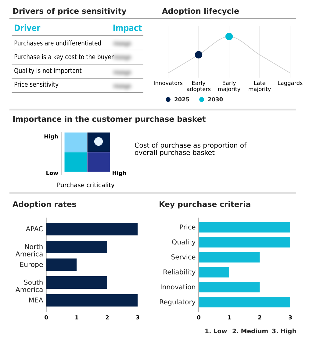
The wafer-level manufacturing equipment market forecasting report includes the adoption lifecycle of the market, covering from the innovator’s stage to the laggard’s stage. It focuses on adoption rates in different regions based on penetration. Furthermore, the wafer-level manufacturing equipment market report also includes key purchase criteria and drivers of price sensitivity to help companies evaluate and develop their market growth analysis strategies.
Customer Landscape of Wafer-level Manufacturing Equipment Industry
Competitive Landscape
Companies are implementing various strategies, such as strategic alliances, wafer-level manufacturing equipment market forecast, partnerships, mergers and acquisitions, geographical expansion, and product/service launches, to enhance their presence in the industry.
Advanced Micro Fabrication Inc - Provides advanced test systems and platforms for comprehensive semiconductor wafer testing, ensuring device integrity and performance at the wafer level.
The industry research and growth report includes detailed analyses of the competitive landscape of the market and information about key companies, including:
- Advanced Micro Fabrication Inc
- Advantest Corp.
- Applied Materials Inc.
- Canon Inc.
- EV Group
- Evatec AG
- KLA Corp.
- Kulicke and Soffa Industries
- Lam Research Corp.
- Nikon Corp.
- Onto Innovation Inc.
- Oxford Instruments plc
- PLASMA THERM
- Screen Holdings Co. Ltd.
- SEMES Co Ltd
- SUSS MICROTEC SE
- Teradyne Inc.
- Tokyo Electron Ltd.
- Ulvac Inc.
- Veeco Instruments Inc.
Qualitative and quantitative analysis of companies has been conducted to help clients understand the wider business environment as well as the strengths and weaknesses of key industry players. Data is qualitatively analyzed to categorize companies as pure play, category-focused, industry-focused, and diversified; it is quantitatively analyzed to categorize companies as dominant, leading, strong, tentative, and weak.
Recent Development and News in Wafer-level manufacturing equipment market
- In August 2024, Tokyo Electron Ltd. and Applied Materials Inc. announced a strategic collaboration to jointly develop next-generation semiconductor manufacturing technologies, focusing on materials engineering and 3D integration.
- In December 2024, Intel Corp. announced a USD 20 billion investment to construct a new state-of-the-art semiconductor fabrication plant in Arizona, aiming to increase domestic manufacturing capacity.
- In February 2025, the European Commission approved a major Austrian program to support AMS Osram in building a new high-volume wafer manufacturing facility, contributing to the European Chips Act objectives.
- In May 2025, Advanced Micro-Fabrication Equipment Inc. reached a key milestone as its 5-nanometer grade etching machine entered the validation phase within the advanced process lines of Taiwan Semiconductor Manufacturing Co.
Dive into Technavio’s robust research methodology, blending expert interviews, extensive data synthesis, and validated models for unparalleled Wafer-level Manufacturing Equipment Market insights. See full methodology.
| Market Scope | |
|---|---|
| Page number | 309 |
| Base year | 2025 |
| Historic period | 2020-2024 |
| Forecast period | 2026-2030 |
| Growth momentum & CAGR | Accelerate at a CAGR of 10.9% |
| Market growth 2026-2030 | USD 101064.3 million |
| Market structure | Fragmented |
| YoY growth 2025-2026(%) | 9.8% |
| Key countries | China, Japan, India, South Korea, Australia, Indonesia, US, Canada, Mexico, Germany, UK, France, Italy, Spain, The Netherlands, Brazil, Argentina, Chile, Saudi Arabia, UAE, South Africa, Israel and Turkey |
| Competitive landscape | Leading Companies, Market Positioning of Companies, Competitive Strategies, and Industry Risks |
Research Analyst Overview
- The wafer-level manufacturing equipment market is defined by relentless innovation in both equipment hardware and software solutions, catering to the distinct needs of foundry, memory, and idm clients. Core processes like deposition and testing are evolving, with extreme ultraviolet (euv) lithography becoming essential for fabricating next-generation gate-all-around (gaa) transistors.
- This requires breakthroughs in etching equipment, including tools for deep reactive-ion etching (drie) and atomic layer etching (ale) to achieve precision. For advanced packaging, technologies like wafer level packaging (wlp) and fan-out wafer level packaging (fowlp) are critical, relying on equipment for creating redistribution layers (rdls), through-silicon vias (tsvs), and executing precise bonding.
- The fabrication of specialized devices such as microelectromechanical systems (mems) and wafer-level optics (wlo) also drives demand for unique processes like backside metallization. Boardroom decisions on capital expenditure are increasingly complex, with firms weighing the massive cost of euv against enhancing existing tools, a choice that directly impacts multi-year budgets.
- The use of advanced atomic layer deposition (ald) and chemical mechanical planarization (cmp) has demonstrated the ability to improve device uniformity by over 20%, justifying the high investment.
What are the Key Data Covered in this Wafer-level Manufacturing Equipment Market Research and Growth Report?
-
What is the expected growth of the Wafer-level Manufacturing Equipment Market between 2026 and 2030?
-
USD 101.06 billion, at a CAGR of 10.9%
-
-
What segmentation does the market report cover?
-
The report is segmented by End-user (Foundry, Memory, and IDM), Product (Wafer fab equipment, and Wafer level packaging), Technology (Photolithography equipment, and Etching equipment), Component (Equipment hardware, and Software solutions) and Geography (APAC, North America, Europe, South America, Middle East and Africa)
-
-
Which regions are analyzed in the report?
-
APAC, North America, Europe, South America and Middle East and Africa
-
-
What are the key growth drivers and market challenges?
-
Exponential growth in high-performance computing and data center infrastructure, Escalating capital intensity and prohibitive equipment procurement costs
-
-
Who are the major players in the Wafer-level Manufacturing Equipment Market?
-
Advanced Micro Fabrication Inc, Advantest Corp., Applied Materials Inc., Canon Inc., EV Group, Evatec AG, KLA Corp., Kulicke and Soffa Industries, Lam Research Corp., Nikon Corp., Onto Innovation Inc., Oxford Instruments plc, PLASMA THERM, Screen Holdings Co. Ltd., SEMES Co Ltd, SUSS MICROTEC SE, Teradyne Inc., Tokyo Electron Ltd., Ulvac Inc. and Veeco Instruments Inc.
-
Market Research Insights
- The wafer-level manufacturing equipment market is driven by intense technological evolution and shifting supply-chain strategies. The adoption of advanced packaging technology, essential for next-generation devices, has improved interconnect performance by over 20% in certain applications. This necessitates sophisticated process control solutions and tools for thin-wafer handling, where new automated systems have reduced breakage rates by 5%.
- As semiconductor fabrication becomes more complex, the integration of AI for yield optimization has become critical, with some fabs reporting a 3% improvement in overall yield. This dynamic environment compels equipment providers to innovate continuously, focusing on solutions that enhance both performance and manufacturing efficiency.
We can help! Our analysts can customize this wafer-level manufacturing equipment market research report to meet your requirements.
 RIA -
RIA -